


Request Quote
(Ships tomorrow)
TLV2548CDWR Equivalent & Substitute Parts
Part Overview
The TLV2548CDWR is a 12-bit Analog to Digital Converter (ADC) manufactured by Texas Instruments, designed for data acquisition applications requiring 8 single-ended inputs with a 200 kSPS sampling rate. The device operates across a 2.7V to 5.5V supply range and features SPI/DSP data interfaces with an integrated multiplexer and sample-and-hold configuration.
This part is designated as Last Time Buy, indicating end-of-life status. Identifying equivalent substitute parts is necessary for design continuity, long-term product support, and ensuring availability for new production runs or design revisions.
Substiute Parts
Key Parameters
| Parameter | Value |
|---|---|
| Resolution | 12 Bit |
| Number of Inputs | 8 |
| Input Type | Single Ended |
| Sampling Rate | 200 kSPS |
| Architecture | SAR (Successive Approximation Register) |
| Data Interface | SPI, DSP |
| Supply Voltage Range | 2.7V ~ 5.5V (Analog & Digital) |
| Operating Temperature | 0°C ~ 70°C |
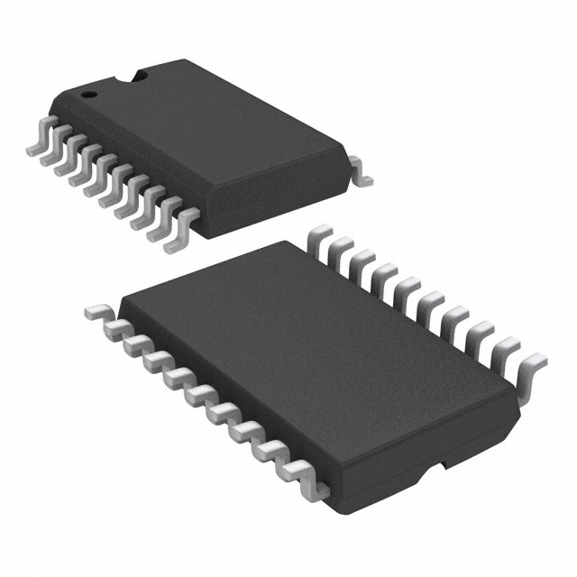
| Package | 20-SOIC (0.295", 7.50mm Width) |
| RoHS Status | ROHS3 Compliant |
Substitute Part Grouping Explanation
Substitution eligibility for the TLV2548CDWR is determined by the following core parameters:
- Resolution: 12-bit ADC architecture
- Channel Count: 8 single-ended inputs
- Sampling Rate: Minimum 200 kSPS capability
- Data Interface: SPI compatibility
- Supply Voltage: Overlapping operating range with 2.7V minimum
- Package Compatibility: Surface mount form factor suitable for PCB integration
- Compliance: ROHS3 and REACH compliance maintained
The ADS7038IRTER qualifies as a manufacturer-recommended substitute based on these criteria, despite differences in package form factor and enhanced performance specifications.
Parameter Comparison
| Parameter | TLV2548CDWR | ADS7038IRTER | Compatibility Notes |
|---|---|---|---|
| Resolution | 12 Bit | 12 Bit | Matched |
| Number of Inputs | 8 | 8 | Matched |
| Input Type | Single Ended | Single Ended | Matched |
| Sampling Rate | 200 kSPS | 1 MSPS | Substitute exceeds requirement |
| Architecture | SAR | SAR | Matched |
| Data Interface | SPI, DSP | SPI | SPI interface matched; DSP interface not available |
| Supply Voltage (Analog) | 2.7V ~ 5.5V | 2.35V ~ 5.5V | Substitute range extends lower |
| Supply Voltage (Digital) | 2.7V ~ 5.5V | 1.65V ~ 5.5V | Substitute range extends lower |
| Operating Temperature | 0°C ~ 70°C | -40°C ~ 125°C | Substitute range exceeds requirement |
| Package | 20-SOIC | 16-WQFN (3x3) | Different form factor; PCB redesign required |
| RoHS Status | ROHS3 Compliant | ROHS3 Compliant | Matched |
Engineering Selection Recommendations
The ADS7038IRTER is designated as the manufacturer-recommended substitute for the TLV2548CDWR. Both devices maintain ROHS3 compliance and REACH unaffected status, ensuring regulatory alignment for production environments.
The ADS7038IRTER offers enhanced performance specifications including higher sampling rate (1 MSPS vs. 200 kSPS), extended operating temperature range (-40°C to 125°C vs. 0°C to 70°C), and lower minimum supply voltage thresholds. These improvements provide design flexibility for applications requiring broader environmental or performance margins.
The primary design consideration is package transition from 20-SOIC to 16-WQFN (3x3), which requires PCB layout modification. The ADS7038IRTER includes additional integrated features (digital window comparator, GPIO, oscillator) not present in the TLV2548CDWR, which may require firmware or application software evaluation.
The TLV2548CDWR's Last Time Buy status necessitates transition planning. The ADS7038IRTER's Active product status ensures long-term availability and continued manufacturer support.
Frequently Asked Questions (FAQ)
Q: Can the ADS7038IRTER directly replace the TLV2548CDWR without PCB modifications?
A: No. The ADS7038IRTER uses a 16-WQFN (3x3) package versus the TLV2548CDWR's 20-SOIC package. PCB layout redesign is required, including footprint changes and signal routing adjustments.
Q: Are the SPI interfaces between these devices compatible?
A: Both devices feature SPI data interfaces. However, the TLV2548CDWR also supports DSP interface, which is not available on the ADS7038IRTER. Applications using only SPI communication will transition without interface modifications.
Q: What are the supply voltage considerations for substitution?
A: The ADS7038IRTER supports lower minimum supply voltages (1.65V digital, 2.35V analog) compared to the TLV2548CDWR (2.7V for both). Existing designs operating at 2.7V or higher are compatible. Designs requiring lower voltage operation benefit from the ADS7038IRTER's extended range.
Q: Does the ADS7038IRTER's higher sampling rate affect design compatibility?
A: The 1 MSPS sampling rate of the ADS7038IRTER exceeds the TLV2548CDWR's 200 kSPS specification. Applications designed for 200 kSPS operation will function correctly with the faster device. No performance degradation occurs from exceeding the original sampling rate requirement.
Q: Are there compliance or certification differences between these parts?
A: Both devices are ROHS3 compliant and REACH unaffected. Regulatory compliance is maintained across the substitution.
Q: What additional features does the ADS7038IRTER provide?
A: The ADS7038IRTER integrates a digital window comparator, GPIO functionality, and an internal oscillator. These features are not present in the TLV2548CDWR and may require evaluation for firmware compatibility or application-specific utility.
Alternative Parts

SJ6012L2TP
Littelfuse Inc.
6 Alternative Parts

JMK107BBJ476MA-RE
Taiyo Yuden
10 Alternative Parts

GMK107BBJ475MA-T
Taiyo Yuden
5 Alternative Parts
SJ6020N2ARP
Littelfuse Inc.
3 Alternative Parts
SJ6025R2ATP
Littelfuse Inc.
4 Alternative Parts

2474-05L
API Delevan Inc.
1 Alternative Parts

4590R-684K
API Delevan Inc.
1 Alternative Parts

CM6560R-334
API Delevan Inc.
1 Alternative Parts

CM6460-104
API Delevan Inc.
1 Alternative Parts

5526-12
API Delevan Inc.
1 Alternative Parts