


Request Quote
(Ships tomorrow)
TLV1543CDB Equivalent & Substitute Parts
Part Overview
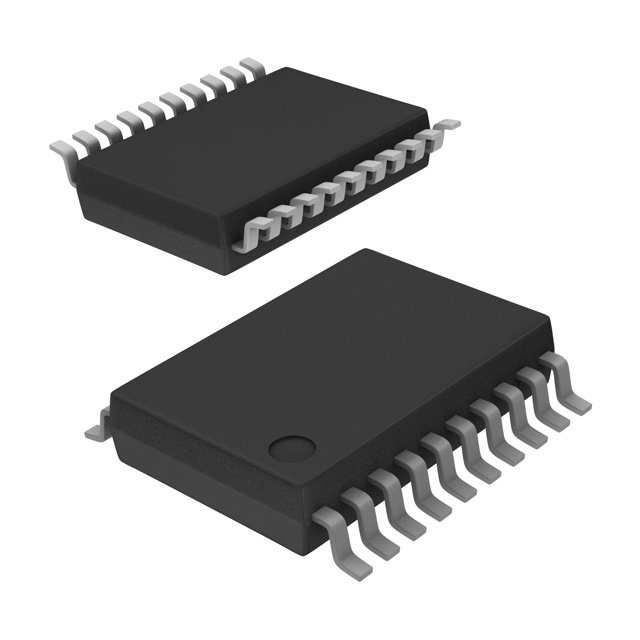
The TLV1543CDB is a 10-bit Analog to Digital Converter (ADC) manufactured by Texas Instruments, designed for data acquisition applications requiring moderate sampling rates and multiple analog inputs. This device features 11 single-ended input channels with a SAR (Successive Approximation Register) architecture and SPI digital interface. The TLV1543CDB is currently in Last Time Buy status, indicating end-of-life production. Identifying equivalent and substitute parts is necessary to ensure design continuity and maintain supply chain reliability for new production runs and long-term product support.
Substiute Parts
Key Parameters
| Parameter | Value |
|---|---|
| Resolution (Bits) | 10 |
| Number of Input Channels | 11 |
| Input Type | Single Ended |
| Sampling Rate | 38 kSPS |
| Architecture | SAR |
| Data Interface | SPI |
| Analog Supply Voltage | 3V to 5.5V |
| Digital Supply Voltage | 3V to 5.5V |
| Operating Temperature Range | 0°C to 70°C |
| Package Type | 20-SSOP |
| RoHS Status | ROHS3 Compliant |
Substitute Part Grouping Explanation
The ADS7956SDBTR qualifies as a manufacturer-recommended substitute for the TLV1543CDB based on the following core substitution criteria:
Matching Parameters:
- Resolution: 10 bits (identical)
- Architecture: SAR (identical)
- Data Interface: SPI (identical)
- Input Type: Single Ended (identical)
- Configuration: MUX-S/H-ADC with 1:1 S/H:ADC ratio (identical)
- Number of A/D Converters: 1 (identical)
- Reference Type: External (identical)
- RoHS Compliance: ROHS3 (identical)
- Mounting Type: Surface Mount (identical)
Allowable Variations:
- Number of Input Channels: 12 (vs. 11 in main part) — additional channel provides design flexibility
- Sampling Rate: 1 MSps (vs. 38 kSps) — higher performance capability maintains backward compatibility
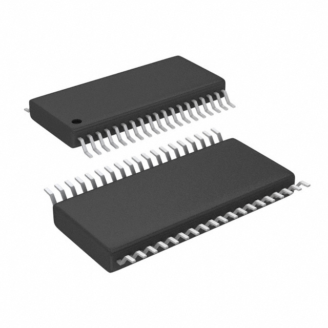
- Package: 38-TSSOP (vs. 20-SSOP) — different form factor requiring PCB layout modification
- Operating Temperature: -40°C to 125°C (vs. 0°C to 70°C) — extended range supports broader applications
- Supply Voltage Range: Analog 2.7V to 5.25V, Digital 1.7V to 5.25V (vs. 3V to 5.5V) — overlapping range with extended lower limit
Parameter Comparison
| Parameter | TLV1543CDB (Main Part) | ADS7956SDBTR (Substitute) |
|---|---|---|
| Manufacturer | Texas Instruments | Texas Instruments |
| Resolution | 10 bits | 10 bits |
| Number of Input Channels | 11 | 12 |
| Input Type | Single Ended | Single Ended |
| Sampling Rate | 38 kSPS | 1 MSPS |
| Architecture | SAR | SAR |
| Data Interface | SPI | SPI |
| Analog Supply Voltage | 3V to 5.5V | 2.7V to 5.25V |
| Digital Supply Voltage | 3V to 5.5V | 1.7V to 5.25V |
| Operating Temperature Range | 0°C to 70°C | -40°C to 125°C |
| Package Type | 20-SSOP | 38-TSSOP |
| RoHS Status | ROHS3 Compliant | ROHS3 Compliant |
| Product Status | Last Time Buy | Active |
Engineering Selection Recommendations
The ADS7956SDBTR is the manufacturer-recommended substitute for the TLV1543CDB. Both devices maintain ROHS3 compliance and are manufactured by Texas Instruments, ensuring consistent quality and reliability standards.
The ADS7956SDBTR offers extended product lifecycle support as an Active product, whereas the TLV1543CDB is in Last Time Buy status. This substitution provides long-term design continuity and supply chain stability.
Key design considerations for substitution:
- Package Change: The transition from 20-SSOP to 38-TSSOP requires PCB layout modification. The 38-TSSOP package is physically larger and has different pin assignments.
- Enhanced Performance: The ADS7956SDBTR provides 1 MSPS sampling rate versus 38 kSPS, offering improved performance headroom for signal acquisition.
- Additional Input Channel: The 12th input channel in the ADS7956SDBTR provides design flexibility for applications requiring expanded analog input capacity.
- Extended Operating Range: The ADS7956SDBTR supports -40°C to 125°C operation, enabling deployment in wider temperature environments compared to the 0°C to 70°C range of the TLV1543CDB.
- Supply Voltage Compatibility: Both devices operate within overlapping supply voltage ranges. The ADS7956SDBTR extends the lower digital supply limit to 1.7V, supporting low-power applications.
Frequently Asked Questions (FAQ)
Q: Can the ADS7956SDBTR directly replace the TLV1543CDB without design changes?
A: Direct pin-for-pin replacement is not possible due to package differences (20-SSOP vs. 38-TSSOP). PCB layout and routing modifications are required. However, the functional compatibility is maintained through identical resolution, architecture, data interface, and input configuration.
Q: What are the main differences between these two devices?
A: The primary differences are package type, sampling rate, number of input channels, and operating temperature range. The ADS7956SDBTR provides higher performance specifications and extended environmental operating conditions.
Q: Is the SPI interface protocol identical between both devices?
A: Both devices use SPI as the data interface with identical configuration (MUX-S/H-ADC, 1:1 ratio). Firmware and software drivers may require verification for specific timing and command sequences, but the interface protocol is compatible.
Q: What is the impact of the additional 12th input channel on system design?
A: The additional input channel in the ADS7956SDBTR provides expanded analog signal acquisition capability. Existing designs using 11 channels can utilize the 12th channel for additional measurements or leave it unused without functional impact.
Q: Are there supply voltage compatibility concerns?
A: Both devices operate within overlapping supply voltage ranges. The ADS7956SDBTR supports lower digital supply voltages (1.7V minimum vs. 3V minimum), making it suitable for low-power applications. Existing 3V to 5.5V supply designs are fully compatible.
Q: How does the extended operating temperature range affect reliability?
A: The ADS7956SDBTR supports -40°C to 125°C operation versus 0°C to 70°C for the TLV1543CDB. This extended range enables deployment in industrial and automotive environments with wider temperature extremes, improving design flexibility for diverse applications.
Q: What packaging considerations should be addressed during substitution?
A: The 38-TSSOP package is larger than the 20-SSOP package. PCB footprint redesign, trace routing modifications, and thermal management considerations may be necessary. Verify component placement constraints and signal integrity requirements for your specific application.
Alternative Parts

SJ6012L2TP
Littelfuse Inc.
6 Alternative Parts

JMK107BBJ476MA-RE
Taiyo Yuden
10 Alternative Parts

GMK107BBJ475MA-T
Taiyo Yuden
5 Alternative Parts
SJ6020N2ARP
Littelfuse Inc.
3 Alternative Parts
SJ6025R2ATP
Littelfuse Inc.
4 Alternative Parts

2474-05L
API Delevan Inc.
1 Alternative Parts

4590R-684K
API Delevan Inc.
1 Alternative Parts

CM6560R-334
API Delevan Inc.
1 Alternative Parts

CM6460-104
API Delevan Inc.
1 Alternative Parts

5526-12
API Delevan Inc.
1 Alternative Parts