


Request Quote
(Ships tomorrow)
TLC542IDWR Equivalent & Substitute Parts
Part Overview
The TLC542IDWR is an 8-bit Analog to Digital Converter (ADC) manufactured by Texas Instruments, designed for data acquisition applications requiring single-ended input multiplexing with SAR (Successive Approximation Register) architecture. This device features 11 input channels, SPI data interface, and operates from a 5V supply. The TLC542IDWR is classified as obsolete, making identification of compatible substitute components essential for ongoing system support, redesigns, and new production requirements.
Substiute Parts
Key Parameters
| Parameter | Value |
|---|---|
| Manufacturer | Texas Instruments |
| Part Number | TLC542IDWR |
| Number of Bits | 8 |
| Sampling Rate | 25 kSPS |
| Number of Inputs | 11 |
| Input Type | Single Ended |
| Data Interface | SPI |
| Architecture | SAR |
| Voltage - Supply, Analog | 5V |
| Voltage - Supply, Digital | 5V |
| Operating Temperature | -40°C to 85°C |
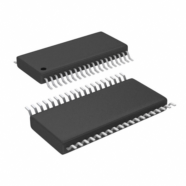
| Package | 20-SOIC |
| Product Status | Obsolete |
| RoHS Status | ROHS3 Compliant |
Substitute Part Grouping Explanation
Substitution of the TLC542IDWR is determined by the following critical parameters:
Core Functional Requirements:
- 8-bit resolution (ADC bit depth)
- SAR architecture (conversion method)
- SPI interface (digital communication protocol)
- Single-ended input configuration
- External reference type
Electrical Compatibility Criteria:
- Supply voltage compatibility (5V operation or wider range including 5V)
- Number of input channels (minimum 11 channels required)
- Sampling rate capability (minimum 25 kSPS)
- Operating temperature range (minimum -40°C to 85°C coverage)
Physical & Compliance Requirements:
- Surface mount packaging
- ROHS3 compliance
- REACH unaffected status
The ADS7960SDBTR meets all core functional requirements and electrical compatibility criteria, with enhanced specifications in sampling rate and operating temperature range, while maintaining backward compatibility with the TLC542IDWR's primary application parameters.
Parameter Comparison
| Parameter | TLC542IDWR | ADS7960SDBTR |
|---|---|---|
| Manufacturer | Texas Instruments | Texas Instruments |
| Number of Bits | 8 | 8 |
| Sampling Rate (Per Second) | 25 kSPS | 1 MSPS |
| Number of Inputs | 11 | 12 |
| Input Type | Single Ended | Single Ended |
| Data Interface | SPI | SPI |
| Architecture | SAR | SAR |
| Reference Type | External | External |
| Voltage - Supply, Analog | 5V | 2.7V to 5.25V |
| Voltage - Supply, Digital | 5V | 1.7V to 5.25V |
| Operating Temperature | -40°C to 85°C | -40°C to 125°C |
| Package / Case | 20-SOIC | 38-TSSOP |
| Product Status | Obsolete | Active |
| RoHS Status | ROHS3 Compliant | ROHS3 Compliant |
| REACH Status | REACH Unaffected | REACH Unaffected |
Engineering Selection Recommendations
The ADS7960SDBTR is the designated Texas Instruments manufacturer substitute for the obsolete TLC542IDWR. Selection of this substitute is supported by the following engineering factors:
Product Status & Availability: The TLC542IDWR is classified as obsolete, whereas the ADS7960SDBTR maintains active product status with current manufacturing and supply chain support.
Regulatory Compliance: Both devices maintain ROHS3 compliance and REACH unaffected status, ensuring compatibility with current environmental and regulatory requirements.
Functional Equivalence: The ADS7960SDBTR preserves the core 8-bit SAR ADC architecture, SPI interface, and single-ended input configuration of the TLC542IDWR. The substitute provides 12 input channels (exceeding the 11-channel requirement) and 1 MSPS sampling rate (exceeding the 25 kSPS requirement), ensuring functional compatibility for applications designed around the original part.
Supply Voltage Flexibility: The ADS7960SDBTR operates across a wider supply voltage range (2.7V to 5.25V analog, 1.7V to 5.25V digital) compared to the fixed 5V requirement of the TLC542IDWR, providing design flexibility for future applications.
Package Consideration: The ADS7960SDBTR uses a 38-TSSOP package versus the 20-SOIC package of the original part. PCB layout redesign is required for direct substitution.
Frequently Asked Questions (FAQ)
Q: Can the ADS7960SDBTR directly replace the TLC542IDWR without PCB modifications?
A: No. The ADS7960SDBTR uses a 38-TSSOP package while the TLC542IDWR uses a 20-SOIC package. PCB layout redesign is required. Pin-to-pin compatibility does not exist between these packages.
Q: Are the SPI interface protocols identical between these two devices?
A: Both devices use SPI as the data interface protocol. Detailed timing and command structure must be verified against the respective device datasheets to ensure software compatibility.
Q: What is the minimum number of input channels required for substitution?
A: The TLC542IDWR provides 11 input channels. The substitute must provide a minimum of 11 channels. The ADS7960SDBTR provides 12 channels, meeting this requirement.
Q: Does the ADS7960SDBTR support the same 5V supply voltage as the TLC542IDWR?
A: Yes. The ADS7960SDBTR operates across 2.7V to 5.25V for analog supply and 1.7V to 5.25V for digital supply, which includes the 5V operating point of the TLC542IDWR.
Q: What is the sampling rate difference between these devices?
A: The TLC542IDWR operates at 25 kSPS, while the ADS7960SDBTR operates at 1 MSPS. The substitute provides 40 times higher sampling rate, which is compatible with applications designed for the lower rate.
Q: Are both devices RoHS compliant?
A: Yes. Both the TLC542IDWR and ADS7960SDBTR are ROHS3 compliant and REACH unaffected, meeting current environmental regulations.
Q: What is the operating temperature range difference?
A: The TLC542IDWR operates from -40°C to 85°C, while the ADS7960SDBTR operates from -40°C to 125°C. The substitute supports a wider temperature range, providing compatibility for extended temperature applications.
Alternative Parts

SJ6012L2TP
Littelfuse Inc.
6 Alternative Parts

JMK107BBJ476MA-RE
Taiyo Yuden
10 Alternative Parts

GMK107BBJ475MA-T
Taiyo Yuden
5 Alternative Parts
SJ6020N2ARP
Littelfuse Inc.
3 Alternative Parts
SJ6025R2ATP
Littelfuse Inc.
4 Alternative Parts

2474-05L
API Delevan Inc.
1 Alternative Parts

4590R-684K
API Delevan Inc.
1 Alternative Parts

CM6560R-334
API Delevan Inc.
1 Alternative Parts

CM6460-104
API Delevan Inc.
1 Alternative Parts

5526-12
API Delevan Inc.
1 Alternative Parts