


Request Quote
(Ships tomorrow)
TLC540IDW Equivalent & Substitute Parts
Part Overview
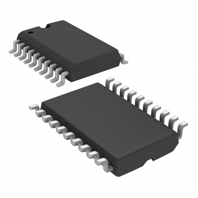
The TLC540IDW is an 8-bit Analog to Digital Converter (ADC) with SAR (Successive Approximation Register) architecture, featuring 11 single-ended inputs and SPI data interface. Manufactured by Texas Instruments in a 20-SOIC package, this component is classified as obsolete. Due to its discontinued status, identifying functionally compatible substitute parts is essential for design continuity and procurement planning.
Substiute Parts
Key Parameters
| Parameter | TLC540IDW |
|---|---|
| Number of Bits | 8 |
| Sampling Rate (Per Second) | 75k |
| Number of Inputs | 11 |
| Input Type | Single Ended |
| Data Interface | SPI |
| Architecture | SAR |
| Reference Type | External, Internal |
| Voltage - Supply, Analog | 5V |
| Voltage - Supply, Digital | 5V |
| Operating Temperature | -40°C ~ 85°C |
| Package / Case | 20-SOIC |
| Product Status | Obsolete |
Substitute Part Grouping Explanation
Substitute parts for the TLC540IDW are identified based on the following core electrical and mechanical parameters:
- Resolution: 8-bit ADC architecture maintained
- Conversion Method: SAR (Successive Approximation Register) architecture
- Input Configuration: Single-ended analog inputs
- Serial Interface: SPI data interface compatibility
- Supply Voltage Compatibility: Operating within or encompassing the original 5V supply range
- Temperature Range: Operating temperature specifications suitable for industrial applications
- Package Type: Surface mount technology with pin-compatible or functionally equivalent packaging
The ADS7960SDBT meets these substitution criteria while offering enhanced specifications including higher sampling rate, expanded input count, and extended temperature range.
Parameter Comparison
| Parameter | TLC540IDW | ADS7960SDBT |
|---|---|---|
| Number of Bits | 8 | 8 |
| Sampling Rate (Per Second) | 75k | 1M |
| Number of Inputs | 11 | 12 |
| Input Type | Single Ended | Single Ended |
| Data Interface | SPI | SPI |
| Architecture | SAR | SAR |
| Reference Type | External, Internal | External |
| Voltage - Supply, Analog | 5V | 2.7V ~ 5.25V |
| Voltage - Supply, Digital | 5V | 1.7V ~ 5.25V |
| Operating Temperature | -40°C ~ 85°C | -40°C ~ 125°C |
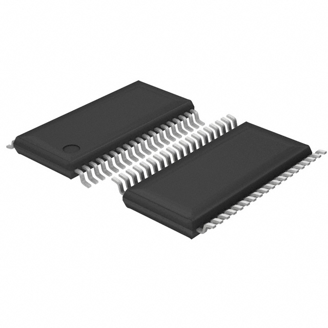
| Package / Case | 20-SOIC | 38-TFSOP |
| Product Status | Obsolete | Active |
| RoHS Status | ROHS3 Compliant | ROHS3 Compliant |
| Moisture Sensitivity Level (MSL) | 1 (Unlimited) | 2 (1 Year) |
Engineering Selection Recommendations
The ADS7960SDBT is the manufacturer-recommended substitute for the obsolete TLC540IDW. Both components maintain identical 8-bit resolution and SAR architecture with SPI interface compatibility. The substitute part is actively manufactured and fully compliant with ROHS3 and REACH requirements, ensuring long-term availability and regulatory compliance.
The ADS7960SDBT provides enhanced performance specifications including 1M sampling rate versus 75k, one additional input channel (12 versus 11), and extended operating temperature range (-40°C to 125°C). The substitute supports a wider analog supply voltage range (2.7V to 5.25V) and reduced digital supply voltage floor (1.7V), offering greater design flexibility.
Package transition from 20-SOIC to 38-TFSOP requires PCB layout modification. The substitute's microPOWER™ series designation indicates optimized power consumption characteristics suitable for battery-powered and low-power applications.
Frequently Asked Questions (FAQ)
Q: Can the ADS7960SDBT directly replace the TLC540IDW without design changes?
A: The ADS7960SDBT maintains functional compatibility in 8-bit resolution, SAR architecture, and SPI interface. However, the package change from 20-SOIC to 38-TFSOP requires PCB layout redesign. Pin assignments must be verified against respective datasheets before implementation.
Q: What are the key differences in supply voltage requirements?
A: The TLC540IDW requires fixed 5V analog and digital supplies. The ADS7960SDBT accepts 2.7V to 5.25V analog supply and 1.7V to 5.25V digital supply, enabling operation in lower-voltage systems and providing greater supply tolerance margins.
Q: How does the increased sampling rate affect system design?
A: The ADS7960SDBT's 1M sampling rate (versus 75k) enables higher-frequency signal acquisition. Applications requiring the original 75k rate can operate the substitute at reduced sampling rates without functional impact. Higher sampling capability does not impose design constraints on lower-frequency applications.
Q: Are there reference voltage configuration differences?
A: The TLC540IDW supports both external and internal reference types. The ADS7960SDBT supports external reference only. Designs utilizing internal reference must be modified to implement external reference circuitry.
Q: What is the impact of the extended temperature range?
A: The ADS7960SDBT operates to 125°C versus 85°C maximum for the TLC540IDW. This extended range provides margin for high-temperature environments but does not restrict use in applications within the original temperature specification.
Q: How does the additional input channel affect system integration?
A: The ADS7960SDBT provides 12 single-ended inputs versus 11 on the TLC540IDW. Existing designs utilizing 11 inputs remain compatible. The additional channel provides expansion capability for future design iterations.
Alternative Parts

SJ6012L2TP
Littelfuse Inc.
6 Alternative Parts

JMK107BBJ476MA-RE
Taiyo Yuden
10 Alternative Parts

GMK107BBJ475MA-T
Taiyo Yuden
5 Alternative Parts
SJ6020N2ARP
Littelfuse Inc.
3 Alternative Parts
SJ6025R2ATP
Littelfuse Inc.
4 Alternative Parts

2474-05L
API Delevan Inc.
1 Alternative Parts

4590R-684K
API Delevan Inc.
1 Alternative Parts

CM6560R-334
API Delevan Inc.
1 Alternative Parts

CM6460-104
API Delevan Inc.
1 Alternative Parts

5526-12
API Delevan Inc.
1 Alternative Parts