


Request Quote
(Ships tomorrow)
TLC2543IDB Equivalent & Substitute Parts
Part Overview
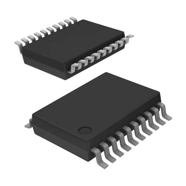
The TLC2543IDB is a 12-bit Analog to Digital Converter (ADC) manufactured by Texas Instruments, designed for data acquisition applications requiring single-ended input processing. This device features 11 input channels with a SAR (Successive Approximation Register) architecture and operates at a sampling rate of 66 kSPS. The TLC2543IDB is currently in Last Time Buy status, indicating end-of-life production. Identifying equivalent and substitute parts is necessary to ensure continued component availability for new designs, production continuity, and long-term system support.
Substiute Parts
Key Parameters
| Parameter | Value |
|---|---|
| Resolution (Bits) | 12 |
| Number of Input Channels | 11 |
| Sampling Rate | 66 kSPS |
| Input Type | Single Ended |
| Data Interface | SPI |
| Architecture | SAR |
| Reference Type | External |
| Analog Supply Voltage | 5V |
| Digital Supply Voltage | 5V |
| Operating Temperature Range | -40°C to 85°C |
| Package Type | 20-SSOP |
| RoHS Status | ROHS3 Compliant |
Substitute Part Grouping Explanation
The ADS7952SBDBTR qualifies as a substitute for the TLC2543IDB based on the following core electrical and mechanical compatibility criteria:
Matching Parameters:
- Resolution: 12-bit (identical)
- Architecture: SAR (identical)
- Input Type: Single Ended (identical)
- Data Interface: SPI (identical)
- Configuration: MUX-S/H-ADC with 1:1 S/H:ADC ratio (identical)
- Number of A/D Converters: 1 (identical)
- Reference Type: External (identical)
- RoHS Status: ROHS3 Compliant (identical)
- Mounting Type: Surface Mount (identical)
Differences Requiring Design Consideration:
- Number of Input Channels: 12 (vs. 11 in TLC2543IDB)
- Sampling Rate: 1 MSPS (vs. 66 kSPS in TLC2543IDB)
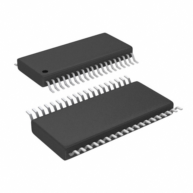
- Package Type: 38-TSSOP (vs. 20-SSOP in TLC2543IDB)
- Supply Voltage Range: 2.7V to 5.25V (vs. fixed 5V in TLC2543IDB)
- Operating Temperature Range: -40°C to 125°C (vs. -40°C to 85°C in TLC2543IDB)
- Product Status: Active (vs. Last Time Buy for TLC2543IDB)
Parameter Comparison
| Parameter | TLC2543IDB | ADS7952SBDBTR |
|---|---|---|
| Manufacturer | Texas Instruments | Texas Instruments |
| Resolution (Bits) | 12 | 12 |
| Number of Input Channels | 11 | 12 |
| Sampling Rate (kSPS) | 66 | 1000 |
| Input Type | Single Ended | Single Ended |
| Data Interface | SPI | SPI |
| Architecture | SAR | SAR |
| Reference Type | External | External |
| Analog Supply Voltage | 5V | 2.7V to 5.25V |
| Digital Supply Voltage | 5V | 1.7V to 5.25V |
| Operating Temperature Range | -40°C to 85°C | -40°C to 125°C |
| Package Type | 20-SSOP | 38-TSSOP |
| RoHS Status | ROHS3 Compliant | ROHS3 Compliant |
| Product Status | Last Time Buy | Active |
Engineering Selection Recommendations
The ADS7952SBDBTR is suitable as a substitute for the TLC2543IDB in applications where the following conditions are met:
-
PCB Layout Compatibility: The transition from 20-SSOP to 38-TSSOP packaging requires PCB redesign. The increased pin count and package footprint must be accommodated in the circuit layout.
-
Supply Voltage Flexibility: The ADS7952SBDBTR accepts a wider supply voltage range (2.7V to 5.25V for analog, 1.7V to 5.25V for digital) compared to the fixed 5V requirement of the TLC2543IDB. Existing 5V supply designs remain compatible.
-
Sampling Rate Capability: The ADS7952SBDBTR operates at 1 MSPS, significantly exceeding the 66 kSPS of the TLC2543IDB. Applications limited to lower sampling rates will function correctly with the substitute.
-
Temperature Range Extension: The ADS7952SBDBTR supports operation to 125°C, providing extended temperature capability beyond the TLC2543IDB's 85°C maximum.
-
Channel Count: The additional input channel (12 vs. 11) in the ADS7952SBDBTR does not create incompatibility; unused channels can remain unconnected.
-
Compliance: Both devices are ROHS3 compliant and REACH unaffected, maintaining regulatory alignment.
Frequently Asked Questions (FAQ)
Q: Can the ADS7952SBDBTR directly replace the TLC2543IDB without PCB modifications?
A: No. The package change from 20-SSOP to 38-TSSOP requires PCB redesign. Pin assignments and footprints differ, necessitating layout modifications and potential schematic updates.
Q: Are the SPI interfaces compatible between these devices?
A: Both devices use SPI data interfaces with identical architecture (SAR, external reference, single-ended inputs). However, pin assignments differ due to package differences. Firmware and hardware interface logic must be verified against device datasheets.
Q: What is the impact of the higher sampling rate on system design?
A: The ADS7952SBDBTR's 1 MSPS sampling rate is backward compatible with applications designed for 66 kSPS operation. No performance degradation occurs; the device simply provides faster conversion capability than required.
Q: Does the wider supply voltage range of the ADS7952SBDBTR affect existing 5V designs?
A: No. The ADS7952SBDBTR operates correctly at 5V supply, matching the TLC2543IDB's supply requirements. The wider range provides design flexibility for future applications.
Q: Are there firmware or driver changes required when switching to the ADS7952SBDBTR?
A: SPI protocol compatibility exists between devices, but register maps, command structures, and timing parameters may differ. Firmware validation against the ADS7952SBDBTR datasheet is required.
Q: What is the significance of the additional input channel in the ADS7952SBDBTR?
A: The ADS7952SBDBTR provides 12 input channels versus 11 in the TLC2543IDB. This additional channel does not create incompatibility; it simply provides expanded input capacity for new designs or future system enhancements.
Alternative Parts

SJ6012L2TP
Littelfuse Inc.
6 Alternative Parts

JMK107BBJ476MA-RE
Taiyo Yuden
10 Alternative Parts

GMK107BBJ475MA-T
Taiyo Yuden
5 Alternative Parts
SJ6020N2ARP
Littelfuse Inc.
3 Alternative Parts
SJ6025R2ATP
Littelfuse Inc.
4 Alternative Parts

2474-05L
API Delevan Inc.
1 Alternative Parts

4590R-684K
API Delevan Inc.
1 Alternative Parts

CM6560R-334
API Delevan Inc.
1 Alternative Parts

CM6460-104
API Delevan Inc.
1 Alternative Parts

5526-12
API Delevan Inc.
1 Alternative Parts