


Request Quote
(Ships tomorrow)
TLC2543CDW Equivalent & Substitute Parts
Part Overview
The TLC2543CDW is a 12-bit Analog to Digital Converter (ADC) manufactured by Texas Instruments, designed for data acquisition applications requiring single-ended input processing. This device features 11 input channels with a SAR (Successive Approximation Register) architecture and operates at a sampling rate of 66 kSPS. The TLC2543CDW is currently in Last Time Buy status, indicating that new production has ceased and existing inventory is being cleared. Finding equivalent or substitute parts is necessary for design continuity, long-term product support, and ensuring availability for future production runs or maintenance applications.
Substiute Parts
Key Parameters
| Parameter | Value |
|---|---|
| Resolution (Bits) | 12 |
| Number of Input Channels | 11 |
| Sampling Rate | 66 kSPS |
| Input Type | Single Ended |
| Data Interface | SPI |
| Architecture | SAR |
| Reference Type | External |
| Analog Supply Voltage | 5V |
| Digital Supply Voltage | 5V |
| Operating Temperature Range | 0°C to 70°C |
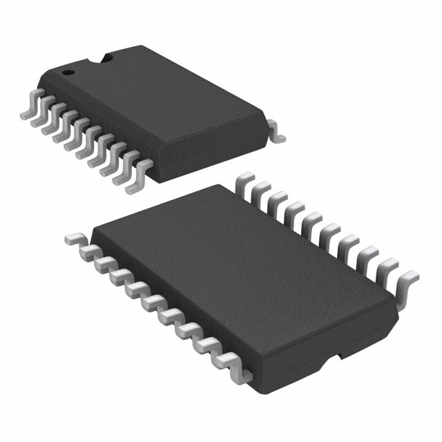
| Package | 20-SOIC |
| RoHS Status | ROHS3 Compliant |
Substitute Part Grouping Explanation
The ADS7952SBDBTR is identified as a manufacturer-recommended substitute for the TLC2543CDW. Substitution eligibility is determined by the following core parameters:
- Resolution: Both devices provide 12-bit conversion accuracy
- Architecture: Both employ SAR-based analog-to-digital conversion
- Data Interface: Both use SPI for serial communication
- Input Configuration: Both feature single-ended input processing with external reference capability
- Converter Count: Both contain a single A/D converter with integrated multiplexer and sample-and-hold circuit
The ADS7952SBDBTR provides enhanced capabilities including 12 input channels (versus 11 on the TLC2543CDW), higher sampling rate (1 MSPS versus 66 kSPS), wider supply voltage range, and extended operating temperature range. These improvements maintain backward compatibility while offering design flexibility for applications requiring higher performance specifications.
Parameter Comparison
| Parameter | TLC2543CDW | ADS7952SBDBTR |
|---|---|---|
| Manufacturer | Texas Instruments | Texas Instruments |
| Resolution (Bits) | 12 | 12 |
| Number of Input Channels | 11 | 12 |
| Sampling Rate (kSPS) | 66 | 1000 |
| Input Type | Single Ended | Single Ended |
| Data Interface | SPI | SPI |
| Architecture | SAR | SAR |
| Reference Type | External | External |
| Analog Supply Voltage Range | 5V (fixed) | 2.7V to 5.25V |
| Digital Supply Voltage Range | 5V (fixed) | 1.7V to 5.25V |
| Operating Temperature Range | 0°C to 70°C | -40°C to 125°C |
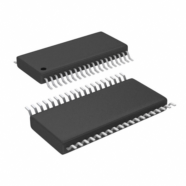
| Package Type | 20-SOIC | 38-TSSOP |
| RoHS Status | ROHS3 Compliant | ROHS3 Compliant |
| REACH Status | REACH Unaffected | REACH Unaffected |
| Product Status | Last Time Buy | Active |
Engineering Selection Recommendations
The ADS7952SBDBTR is suitable as a substitute for the TLC2543CDW based on the following engineering criteria:
Compliance and Regulatory Status: Both devices maintain ROHS3 compliance and REACH unaffected status, ensuring regulatory alignment for industrial and commercial applications.
Product Lifecycle: The ADS7952SBDBTR carries Active product status, providing long-term availability and continued manufacturer support. This addresses the obsolescence risk associated with the TLC2543CDW's Last Time Buy designation.
Functional Compatibility: Core ADC functionality remains consistent between devices. Both employ 12-bit SAR architecture with SPI interface and external reference configuration, enabling direct functional replacement in most applications.
Design Considerations: PCB layout modifications are required due to package change from 20-SOIC to 38-TSSOP. The increased pin count (38 versus 20) accommodates the additional input channel and may require board redesign. Supply voltage flexibility in the ADS7952SBDBTR allows operation across wider input ranges, though fixed 5V operation remains supported.
Frequently Asked Questions (FAQ)
Q: Can the ADS7952SBDBTR directly replace the TLC2543CDW without firmware changes?
A: The SPI interface and 12-bit data format are compatible. However, the additional input channel (12 versus 11) and different pin assignments require firmware updates to the multiplexer control logic and PCB layout modifications.
Q: What are the package differences between these devices?
A: The TLC2543CDW uses a 20-pin SOIC package (0.295" width), while the ADS7952SBDBTR uses a 38-pin TSSOP package (0.173" width). The TSSOP package is physically smaller in width but contains more pins, requiring complete PCB redesign.
Q: Are there temperature range limitations when substituting?
A: The TLC2543CDW operates from 0°C to 70°C, while the ADS7952SBDBTR operates from -40°C to 125°C. If your application requires operation below 0°C or above 70°C, the ADS7952SBDBTR provides extended capability. For standard industrial temperature ranges, both devices are compatible.
Q: What supply voltage considerations apply to substitution?
A: The TLC2543CDW requires fixed 5V supplies for both analog and digital domains. The ADS7952SBDBTR accepts 2.7V to 5.25V for analog supply and 1.7V to 5.25V for digital supply, providing greater flexibility. Designs using fixed 5V supplies remain fully compatible with the substitute device.
Q: How does the sampling rate difference affect substitution?
A: The ADS7952SBDBTR provides 1 MSPS sampling rate compared to 66 kSPS for the TLC2543CDW. This higher performance is backward compatible—applications designed for 66 kSPS operation function correctly with the faster device. No firmware changes are required to accommodate the higher sampling capability.
Q: Are there moisture sensitivity or handling differences?
A: The TLC2543CDW has MSL Level 1 (unlimited shelf life), while the ADS7952SBDBTR has MSL Level 2 (1-year shelf life). Standard moisture control procedures for Level 2 components apply to the substitute device.
Alternative Parts

SJ6012L2TP
Littelfuse Inc.
6 Alternative Parts

JMK107BBJ476MA-RE
Taiyo Yuden
10 Alternative Parts

GMK107BBJ475MA-T
Taiyo Yuden
5 Alternative Parts
SJ6020N2ARP
Littelfuse Inc.
3 Alternative Parts
SJ6025R2ATP
Littelfuse Inc.
4 Alternative Parts

2474-05L
API Delevan Inc.
1 Alternative Parts

4590R-684K
API Delevan Inc.
1 Alternative Parts

CM6560R-334
API Delevan Inc.
1 Alternative Parts

CM6460-104
API Delevan Inc.
1 Alternative Parts

5526-12
API Delevan Inc.
1 Alternative Parts