


Request Quote
(Ships tomorrow)
TLC1542CDWR Equivalent & Substitute Parts
Part Overview
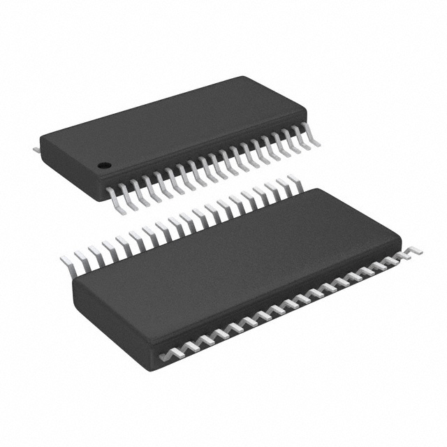
The TLC1542CDWR is a 10-bit Analog to Digital Converter (ADC) manufactured by Texas Instruments, designed for data acquisition applications requiring single-ended input multiplexing with SPI interface. The device features 11 input channels, a SAR (Successive Approximation Register) architecture, and operates from a 5V supply. Currently classified as Last Time Buy, alternative components may be required for new designs or when inventory becomes unavailable.
Substiute Parts
Key Parameters
| Parameter | Value |
|---|---|
| Resolution (Bits) | 10 |
| Number of Input Channels | 11 |
| Sampling Rate | 38 kSPS |
| Architecture | SAR |
| Data Interface | SPI |
| Input Type | Single Ended |
| Analog Supply Voltage | 5V |
| Digital Supply Voltage | 5V |
| Package | 20-SOIC |
| Operating Temperature Range | 0°C to 70°C |
Substitute Part Grouping Explanation
Substitution of the TLC1542CDWR is determined by the following core parameters:
- 10-bit resolution requirement
- SAR architecture for deterministic conversion timing
- SPI serial interface compatibility
- Single-ended input configuration
- External reference voltage capability
The ADS7956SDBTR qualifies as a substitute based on matching these fundamental specifications. While the substitute offers enhanced performance characteristics (higher sampling rate, wider supply voltage range, extended temperature range), it maintains functional compatibility through identical resolution, architecture, interface protocol, and input type. The increase in input channels (12 vs. 11) and different package form factor (38-TSSOP vs. 20-SOIC) represent design trade-offs that must be evaluated for specific application requirements.
Parameter Comparison
| Parameter | TLC1542CDWR | ADS7956SDBTR |
|---|---|---|
| Manufacturer | Texas Instruments | Texas Instruments |
| Resolution | 10 Bit | 10 Bit |
| Number of Inputs | 11 | 12 |
| Sampling Rate | 38 kSPS | 1 MSPS |
| Architecture | SAR | SAR |
| Data Interface | SPI | SPI |
| Input Type | Single Ended | Single Ended |
| Reference Type | External | External |
| Analog Supply Voltage | 5V | 2.7V to 5.25V |
| Digital Supply Voltage | 5V | 1.7V to 5.25V |
| Operating Temperature | 0°C to 70°C | -40°C to 125°C |
| Package | 20-SOIC | 38-TSSOP |
| RoHS Status | ROHS3 Compliant | ROHS3 Compliant |
| REACH Status | REACH Unaffected | REACH Unaffected |
Engineering Selection Recommendations
Selection between TLC1542CDWR and ADS7956SDBTR depends on application-specific constraints:
The TLC1542CDWR remains the primary choice for existing designs with established PCB layouts, thermal profiles limited to 0°C to 70°C, and supply voltage fixed at 5V. Its Last Time Buy status indicates limited future availability; designs currently in production should maintain inventory or initiate migration planning.
The ADS7956SDBTR is suitable for new designs requiring extended operating temperature range (-40°C to 125°C), flexible supply voltage operation (2.7V to 5.25V analog, 1.7V to 5.25V digital), or higher sampling rates (1 MSPS vs. 38 kSPS). The additional input channel (12 vs. 11) may reduce external multiplexing requirements. PCB redesign is necessary due to package change from 20-SOIC to 38-TSSOP.
Both devices maintain ROHS3 compliance and REACH unaffected status, meeting current regulatory requirements.
Frequently Asked Questions (FAQ)
Q: Can ADS7956SDBTR directly replace TLC1542CDWR on existing PCBs?
A: No. The package change from 20-SOIC to 38-TSSOP requires PCB redesign. Pin assignments differ between the two devices. Schematic and layout modifications are mandatory.
Q: Are the SPI interfaces fully compatible?
A: Both devices use SPI protocol for data communication. However, timing parameters, command structures, and register definitions must be verified against respective datasheets. Firmware modifications may be required.
Q: What is the impact of the 12-channel vs. 11-channel difference?
A: The ADS7956SDBTR provides one additional input channel. Existing designs using 11 channels can utilize the extra channel for additional signal acquisition or leave it unused. No functional incompatibility exists.
Q: Why does ADS7956SDBTR have a higher sampling rate?
A: The ADS7956SDBTR incorporates enhanced analog circuitry enabling 1 MSPS operation compared to 38 kSPS for TLC1542CDWR. Applications requiring faster conversion rates benefit from this improvement. Slower sampling rates remain achievable through firmware control.
Q: Are supply voltage differences critical?
A: TLC1542CDWR requires fixed 5V supplies. ADS7956SDBTR accepts 2.7V to 5.25V analog and 1.7V to 5.25V digital supplies, enabling operation in systems with lower or variable supply voltages. Existing 5V designs remain compatible with ADS7956SDBTR.
Q: What is the MSL (Moisture Sensitivity Level) difference?
A: TLC1542CDWR has MSL 1 (unlimited shelf life). ADS7956SDBTR has MSL 2 (1-year shelf life). Storage and handling procedures differ; ADS7956SDBTR requires moisture control during extended storage.
Alternative Parts

SJ6012L2TP
Littelfuse Inc.
6 Alternative Parts

JMK107BBJ476MA-RE
Taiyo Yuden
10 Alternative Parts

GMK107BBJ475MA-T
Taiyo Yuden
5 Alternative Parts
SJ6020N2ARP
Littelfuse Inc.
3 Alternative Parts
SJ6025R2ATP
Littelfuse Inc.
4 Alternative Parts

2474-05L
API Delevan Inc.
1 Alternative Parts

4590R-684K
API Delevan Inc.
1 Alternative Parts

CM6560R-334
API Delevan Inc.
1 Alternative Parts

CM6460-104
API Delevan Inc.
1 Alternative Parts

5526-12
API Delevan Inc.
1 Alternative Parts