


Request Quote
(Ships tomorrow)
THS1215IPW Equivalent & Substitute Parts
Part Overview
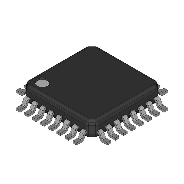
The THS1215IPW is a 12-bit pipelined analog-to-digital converter manufactured by Texas Instruments, designed for single-channel differential input applications. This device operates at a 15 MSPS sampling rate with external or internal reference capability and is housed in a 28-TSSOP surface mount package.
The THS1215IPW is classified as obsolete. Locating equivalent or substitute components is necessary to support legacy system maintenance, design updates, or when original inventory becomes unavailable. Substitute parts must maintain functional compatibility across key electrical parameters including resolution, sampling rate, input configuration, and supply voltage specifications.
Substiute Parts
Key Parameters
| Parameter | THS1215IPW |
|---|---|
| Number of Bits | 12 |
| Sampling Rate (Per Second) | 15 MSPS |
| Number of Inputs | 1 |
| Input Type | Differential |
| Data Interface | Parallel |
| Architecture | Pipelined |
| Reference Type | External, Internal |
| Voltage - Supply, Analog | 3V ~ 3.6V |
| Voltage - Supply, Digital | 3V ~ 3.6V |
| Operating Temperature | -40°C ~ 85°C |
| Package / Case | 28-TSSOP |
| Mounting Type | Surface Mount |
| Product Status | Obsolete |
Substitute Part Grouping Explanation
Substitution of the THS1215IPW is evaluated based on the following critical parameters that define functional compatibility:
Resolution & Sampling Rate: The THS1215IPW operates at 12 bits with a 15 MSPS sampling rate. Substitute parts must support equivalent or superior resolution and sampling performance to maintain signal fidelity in the target application.
Input Configuration: Single differential input with parallel data interface and pipelined architecture are core functional requirements. Substitute parts must preserve this configuration.
Supply Voltage Compatibility: Both analog and digital supply voltages operate within the 3V to 3.6V range. Substitute parts must support this voltage specification to ensure direct integration into existing power distribution networks.
Operating Temperature Range: The -40°C to 85°C operating range defines the thermal envelope. Substitute parts must meet or exceed this specification.
Package & Mounting: Surface mount technology with compatible pinout and package footprint is required for PCB integration without redesign.
Parameter Comparison
| Parameter | THS1215IPW | ADC14L020CIVY/NOPB | Compatibility Notes |
|---|---|---|---|
| Number of Bits | 12 | 14 | Substitute offers higher resolution |
| Sampling Rate (Per Second) | 15 MSPS | 20 MSPS | Substitute offers higher sampling rate |
| Number of Inputs | 1 | 1 | Matched |
| Input Type | Differential | Differential | Matched |
| Data Interface | Parallel | Parallel | Matched |
| Architecture | Pipelined | Pipelined | Matched |
| Reference Type | External, Internal | External, Internal | Matched |
| Voltage - Supply, Analog | 3V ~ 3.6V | 3V ~ 3.6V | Matched |
| Voltage - Supply, Digital | 3V ~ 3.6V | 3V ~ 3.6V | Matched |
| Operating Temperature | -40°C ~ 85°C | -40°C ~ 85°C | Matched |
| Package / Case | 28-TSSOP | 32-LQFP | Different package; PCB redesign required |
| Product Status | Obsolete | Active | Substitute is in active production |
Engineering Selection Recommendations
The ADC14L020CIVY/NOPB is a functional substitute for the THS1215IPW based on matched electrical specifications across resolution, sampling rate, input configuration, supply voltage, and operating temperature range. The substitute device is currently in active production status, ensuring long-term availability and supply chain stability compared to the obsolete THS1215IPW.
The primary design consideration is package compatibility. The THS1215IPW uses a 28-TSSOP package, while the ADC14L020CIVY/NOPB uses a 32-LQFP package. This difference requires PCB layout modification and footprint redesign. Pin-to-pin functional mapping must be verified against device datasheets prior to implementation.
The ADC14L020CIVY/NOPB offers enhanced performance specifications with 14-bit resolution and 20 MSPS sampling rate, providing headroom for signal processing applications that may benefit from increased dynamic range and conversion speed.
Frequently Asked Questions (FAQ)
Q: Can the ADC14L020CIVY/NOPB directly replace the THS1215IPW without PCB modification?
A: No. The package types differ (28-TSSOP versus 32-LQFP), requiring PCB footprint redesign and layout changes. Pin assignments must be verified against manufacturer datasheets to ensure correct signal routing.
Q: What are the key electrical compatibility factors between these devices?
A: Both devices share identical supply voltage ranges (3V to 3.6V), operating temperature range (-40°C to 85°C), input configuration (single differential), data interface (parallel), and architecture (pipelined). These matched parameters establish functional compatibility at the system level.
Q: Does the higher bit resolution of the ADC14L020CIVY/NOPB affect compatibility?
A: The 14-bit resolution of the substitute is a superset of the 12-bit THS1215IPW specification. Applications designed for 12-bit data can operate with 14-bit output by masking or truncating the additional bits if necessary. This represents an enhancement rather than a compatibility issue.
Q: Is the increased sampling rate of the ADC14L020CIVY/NOPB a concern?
A: The 20 MSPS sampling rate of the substitute exceeds the 15 MSPS specification of the original device. This provides additional performance margin and does not create compatibility constraints for applications designed around the lower sampling rate.
Q: What compliance certifications apply to the substitute part?
A: The ADC14L020CIVY/NOPB carries ECCN 3A991C3 and HTSUS 8542.39.0001 classifications. Verify these designations against your application's regulatory and export requirements prior to procurement.
Alternative Parts

SJ6012L2TP
Littelfuse Inc.
6 Alternative Parts

JMK107BBJ476MA-RE
Taiyo Yuden
10 Alternative Parts

GMK107BBJ475MA-T
Taiyo Yuden
5 Alternative Parts
SJ6020N2ARP
Littelfuse Inc.
3 Alternative Parts
SJ6025R2ATP
Littelfuse Inc.
4 Alternative Parts

2474-05L
API Delevan Inc.
1 Alternative Parts

4590R-684K
API Delevan Inc.
1 Alternative Parts

CM6560R-334
API Delevan Inc.
1 Alternative Parts

CM6460-104
API Delevan Inc.
1 Alternative Parts

5526-12
API Delevan Inc.
1 Alternative Parts