


Request Quote
(Ships tomorrow)
THS1215IDW Equivalent & Substitute Parts
Part Overview
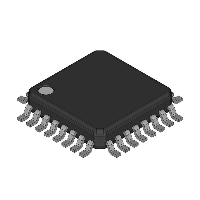
The THS1215IDW is a 12-bit pipelined analog-to-digital converter manufactured by Texas Instruments, housed in a 28-SOIC surface mount package. This device features a single differential input with a 15 MSPS sampling rate and operates on 3V to 3.6V supply voltage for both analog and digital domains. The THS1215IDW is classified as obsolete, making identification of functionally compatible alternatives essential for ongoing system support and new design implementations.
Substiute Parts
Key Parameters
| Parameter | Value |
|---|---|
| Manufacturer Part Number | THS1215IDW |
| Manufacturer | Texas Instruments |
| Number of Bits | 12 |
| Sampling Rate (Per Second) | 15 MSPS |
| Number of Inputs | 1 |
| Input Type | Differential |
| Architecture | Pipelined |
| Data Interface | Parallel |
| Voltage - Supply, Analog | 3V ~ 3.6V |
| Voltage - Supply, Digital | 3V ~ 3.6V |
| Operating Temperature | -40°C ~ 85°C |
| Package / Case | 28-SOIC (0.295", 7.50mm Width) |
| Mounting Type | Surface Mount |
| Product Status | Obsolete |
| RoHS Status | ROHS3 Compliant |
Substitute Part Grouping Explanation
Substitution of the THS1215IDW is determined by the following critical parameters:
- Architecture & Configuration: Pipelined ADC with single differential input and parallel data interface
- Resolution & Sampling Rate: 12-bit resolution at 15 MSPS minimum
- Supply Voltage Compatibility: 3V to 3.6V operation for both analog and digital supplies
- Input Characteristics: Single differential input channel
- Operating Temperature Range: -40°C to 85°C
- Compliance Requirements: ROHS3 compliance and surface mount packaging
The ADC14L020CIVY/NOPB qualifies as a substitute based on matching or exceeding these core parameters while maintaining functional compatibility in pipelined ADC applications.
Parameter Comparison
| Parameter | THS1215IDW | ADC14L020CIVY/NOPB |
|---|---|---|
| Manufacturer | Texas Instruments | National Semiconductor |
| Number of Bits | 12 | 14 |
| Sampling Rate (Per Second) | 15 MSPS | 20 MSPS |
| Number of Inputs | 1 | 1 |
| Input Type | Differential | Differential |
| Architecture | Pipelined | Pipelined |
| Data Interface | Parallel | Parallel |
| Voltage - Supply, Analog | 3V ~ 3.6V | 3V ~ 3.6V |
| Voltage - Supply, Digital | 3V ~ 3.6V | 3V ~ 3.6V |
| Operating Temperature | -40°C ~ 85°C | -40°C ~ 85°C |
| Package / Case | 28-SOIC | 32-LQFP |
| Mounting Type | Surface Mount | Surface Mount |
| Product Status | Obsolete | Active |
| RoHS Status | ROHS3 Compliant | Not specified |
Engineering Selection Recommendations
The ADC14L020CIVY/NOPB serves as a functional substitute for the obsolete THS1215IDW in applications requiring pipelined analog-to-digital conversion. The substitute part offers enhanced specifications with 14-bit resolution and 20 MSPS sampling rate, exceeding the original 12-bit, 15 MSPS performance. Both devices maintain identical supply voltage ranges (3V to 3.6V) and operating temperature specifications (-40°C to 85°C), ensuring thermal and electrical compatibility.
The primary design consideration is package transition from 28-SOIC to 32-LQFP, which requires PCB layout modification. The ADC14L020CIVY/NOPB maintains active product status, ensuring long-term availability and supply chain stability compared to the obsolete THS1215IDW.
Frequently Asked Questions (FAQ)
Q: Can the ADC14L020CIVY/NOPB directly replace the THS1215IDW without circuit modifications?
A: The ADC14L020CIVY/NOPB is functionally compatible but requires PCB layout changes due to package differences (28-SOIC versus 32-LQFP). Pin assignments and signal routing must be verified against device datasheets before implementation.
Q: What are the key advantages of substituting to the ADC14L020CIVY/NOPB?
A: The substitute provides higher resolution (14-bit versus 12-bit) and faster sampling rate (20 MSPS versus 15 MSPS) while maintaining identical supply voltage and temperature operating ranges. Active product status ensures continued availability and support.
Q: Are there any electrical compatibility concerns between these devices?
A: Both devices operate on 3V to 3.6V supply voltage for analog and digital domains and share identical temperature specifications. Differential input configuration and parallel data interface are consistent across both parts.
Q: What is the impact of package change from 28-SOIC to 32-LQFP?
A: Package transition requires PCB redesign for footprint accommodation and trace routing. Pin count increases from 28 to 32, necessitating verification of unused pins and their proper handling in the application circuit.
Q: Is the ADC14L020CIVY/NOPB suitable for legacy system repairs?
A: Yes, the ADC14L020CIVY/NOPB is suitable for legacy system support applications. However, PCB modification is mandatory due to package differences. Active product status provides long-term supply availability for ongoing maintenance requirements.
Alternative Parts

SJ6012L2TP
Littelfuse Inc.
6 Alternative Parts

JMK107BBJ476MA-RE
Taiyo Yuden
10 Alternative Parts

GMK107BBJ475MA-T
Taiyo Yuden
5 Alternative Parts
SJ6020N2ARP
Littelfuse Inc.
3 Alternative Parts
SJ6025R2ATP
Littelfuse Inc.
4 Alternative Parts

2474-05L
API Delevan Inc.
1 Alternative Parts

4590R-684K
API Delevan Inc.
1 Alternative Parts

CM6560R-334
API Delevan Inc.
1 Alternative Parts

CM6460-104
API Delevan Inc.
1 Alternative Parts

5526-12
API Delevan Inc.
1 Alternative Parts