


Request Quote
(Ships tomorrow)
THS1030CDW Equivalent & Substitute Parts
Part Overview
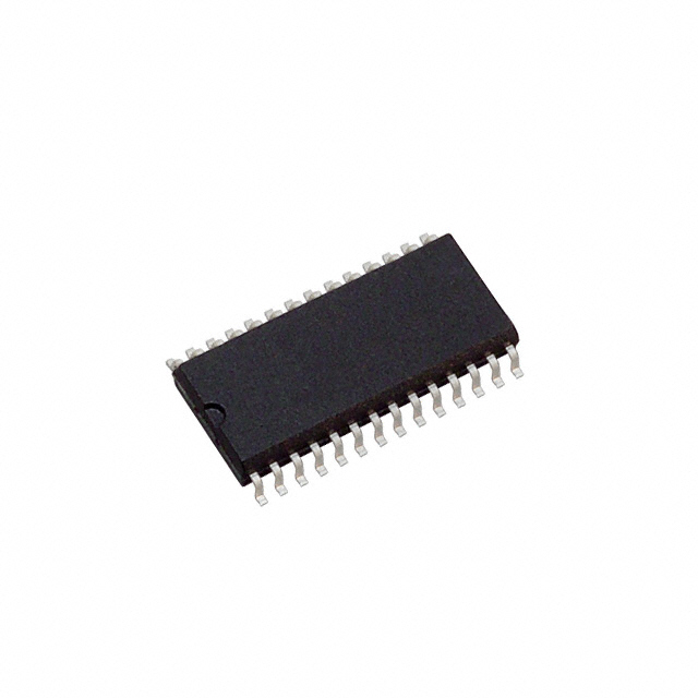
The THS1030CDW is a 10-bit pipelined analog-to-digital converter manufactured by Texas Instruments, designed for data acquisition applications requiring single or differential input processing. This device operates with a 30 MHz sampling rate and supports both 3V to 5.5V analog and digital supply voltages. The THS1030CDW is classified as obsolete, making identification of functionally equivalent alternatives essential for ongoing system support, redesigns, and production continuity.
Substiute Parts
Key Parameters
| Parameter | Value |
|---|---|
| Manufacturer Part Number | THS1030CDW |
| Manufacturer | Texas Instruments |
| Number of Bits | 10 |
| Sampling Rate (Per Second) | 30 MHz |
| Number of Inputs | 1 |
| Input Type | Differential, Single Ended |
| Data Interface | Parallel |
| Architecture | Pipelined |
| Voltage - Supply, Analog | 3V ~ 5.5V |
| Voltage - Supply, Digital | 3V ~ 5.5V |
| Operating Temperature | 0°C ~ 70°C |
| Package / Case | 28-SOIC (0.295", 7.50mm Width) |
| Mounting Type | Surface Mount |
| Product Status | Obsolete |
| RoHS Status | ROHS3 Compliant |
Substitute Part Grouping Explanation
Substitution of the THS1030CDW is determined by the following critical parameters:
- Resolution: 10-bit conversion capability
- Sampling Rate: Minimum 30 MHz performance
- Input Configuration: Support for differential and single-ended inputs
- Architecture: Pipelined ADC topology
- Supply Voltage Compatibility: Analog and digital supply ranges
- Data Interface: Parallel output structure
- Compliance: ROHS3 compliance and REACH unaffected status
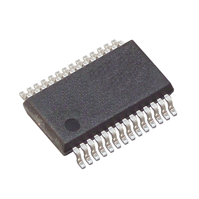
The ADS825E qualifies as a manufacturer-recommended substitute based on matching these core electrical and functional specifications. While package and operating temperature ranges differ, the electrical performance parameters and compliance certifications align with substitution criteria for this product category.
Parameter Comparison
| Parameter | THS1030CDW | ADS825E |
|---|---|---|
| Manufacturer | Texas Instruments | Texas Instruments |
| Number of Bits | 10 | 10 |
| Sampling Rate (Per Second) | 30 MHz | 40 MHz |
| Number of Inputs | 1 | 1 |
| Input Type | Differential, Single Ended | Differential, Single Ended |
| Data Interface | Parallel | Parallel |
| Architecture | Pipelined | Pipelined |
| Reference Type | External, Internal | External, Internal |
| Voltage - Supply, Analog | 3V ~ 5.5V | 5V |
| Voltage - Supply, Digital | 3V ~ 5.5V | 5V |
| Operating Temperature | 0°C ~ 70°C | -40°C ~ 85°C |
| Package / Case | 28-SOIC (0.295", 7.50mm Width) | 28-SSOP (0.209", 5.30mm Width) |
| Mounting Type | Surface Mount | Surface Mount |
| Product Status | Obsolete | Active |
| RoHS Status | ROHS3 Compliant | ROHS3 Compliant |
Engineering Selection Recommendations
The ADS825E is designated as the manufacturer-recommended substitute for the THS1030CDW. Both devices maintain ROHS3 compliance and REACH unaffected status, ensuring regulatory alignment for production applications.
The ADS825E offers active product status, providing ongoing manufacturer support and availability compared to the obsolete THS1030CDW. The substitute device delivers higher sampling rate performance (40 MHz versus 30 MHz), supporting applications requiring increased throughput.
Supply voltage specifications differ: the ADS825E operates at fixed 5V for both analog and digital supplies, whereas the THS1030CDW supports a wider range (3V to 5.5V). System designs must confirm 5V supply availability when implementing the ADS825E.
Package geometry differs between devices. The ADS825E uses 28-SSOP packaging (5.30mm width) compared to the THS1030CDW 28-SOIC packaging (7.50mm width). PCB layout modifications are required for package transition.
Operating temperature range expansion (−40°C to 85°C for ADS825E versus 0°C to 70°C for THS1030CDW) provides broader environmental operating capability with the substitute device.
Frequently Asked Questions (FAQ)
Q: Can the ADS825E directly replace the THS1030CDW without circuit modifications?
A: Electrical functionality is compatible based on matching 10-bit resolution, pipelined architecture, and parallel data interface. However, package geometry differs (28-SSOP versus 28-SOIC), requiring PCB layout redesign. Supply voltage must be confirmed at 5V for the ADS825E.
Q: What are the key differences between these devices?
A: The primary differences are product status (ADS825E is active; THS1030CDW is obsolete), sampling rate (40 MHz versus 30 MHz), supply voltage specification (fixed 5V versus 3V–5.5V range), operating temperature range (−40°C to 85°C versus 0°C to 70°C), and package type (28-SSOP versus 28-SOIC).
Q: Is the ADS825E suitable for applications requiring the 3V to 5.5V supply range of the THS1030CDW?
A: No. The ADS825E requires fixed 5V supply voltage. Applications dependent on the wider 3V to 5.5V supply range of the THS1030CDW must confirm system power architecture supports 5V operation before substitution.
Q: What compliance certifications apply to both devices?
A: Both the THS1030CDW and ADS825E are ROHS3 compliant and REACH unaffected, meeting regulatory requirements for industrial and commercial applications.
Q: Does the higher sampling rate of the ADS825E affect system design?
A: The 40 MHz sampling rate of the ADS825E exceeds the 30 MHz specification of the THS1030CDW. System designs must confirm that downstream signal processing and data handling components support the increased data rate.
Alternative Parts

SJ6012L2TP
Littelfuse Inc.
6 Alternative Parts

JMK107BBJ476MA-RE
Taiyo Yuden
10 Alternative Parts

GMK107BBJ475MA-T
Taiyo Yuden
5 Alternative Parts
SJ6020N2ARP
Littelfuse Inc.
3 Alternative Parts
SJ6025R2ATP
Littelfuse Inc.
4 Alternative Parts

2474-05L
API Delevan Inc.
1 Alternative Parts

4590R-684K
API Delevan Inc.
1 Alternative Parts

CM6560R-334
API Delevan Inc.
1 Alternative Parts

CM6460-104
API Delevan Inc.
1 Alternative Parts

5526-12
API Delevan Inc.
1 Alternative Parts