


Request Quote
(Ships tomorrow)
SY89873LMI Equivalent & Substitute Parts
Part Overview
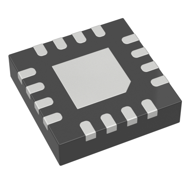
The SY89873LMI is a Clock Fanout Buffer (Distribution), Divider IC manufactured by Microchip Technology, designed for high-speed clock distribution applications up to 2 GHz. This device features a 1:3 input-to-output ratio with differential input and output capabilities, supporting multiple input standards (CML, HSTL, LVDS, LVPECL) and LVDS output. The SY89873LMI is currently discontinued at DiGi Electronics, necessitating identification of equivalent substitute parts for ongoing design requirements and component procurement.
Substiute Parts
Key Parameters
| Parameter | Value |
|---|---|
| Manufacturer | Microchip Technology |
| Part Number | SY89873LMI |
| Category | Clock/Timing |
| Type | Fanout Buffer (Distribution), Divider |
| Ratio - Input:Output | 1:3 |
| Frequency - Max | 2 GHz |
| Voltage - Supply | 2.97V ~ 3.63V |
| Operating Temperature | -40°C ~ 85°C |
| Package / Case | 16-VFQFN Exposed Pad, 16-MLF® |
| Mounting Type | Surface Mount |
| Input Standards | CML, HSTL, LVDS, LVPECL |
| Output Standard | LVDS |
Substitute Part Grouping Explanation
Substitute parts for the SY89873LMI are classified based on the following critical parameters that determine functional compatibility:
Direct Substitutes (Identical Specifications):
- Input:Output Ratio: 1:3
- Maximum Frequency: 2 GHz
- Supply Voltage Range: 2.97V ~ 3.63V
- Operating Temperature Range: -40°C ~ 85°C
- Package: 16-VFQFN Exposed Pad, 16-MLF® (3x3)
- Input/Output Standards: CML, HSTL, LVDS, LVPECL input; LVDS output
Parametric Equivalents (Functional Differences):
- Parts with identical electrical specifications except for Input:Output ratio or other functional parameters may serve as alternatives depending on application requirements.
Parameter Comparison
| Parameter | SY89873LMI | SY89873LMG | SY89876LMG |
|---|---|---|---|
| Manufacturer | Microchip Technology | Microchip Technology | Microchip Technology |
| Category | Clock/Timing | Clock/Timing | Clock/Timing |
| Type | Fanout Buffer (Distribution), Divider | Fanout Buffer (Distribution), Divider | Fanout Buffer (Distribution), Divider |
| Ratio - Input:Output | 1:3 | 1:3 | 1:2 |
| Frequency - Max | 2 GHz | 2 GHz | 2 GHz |
| Voltage - Supply | 2.97V ~ 3.63V | 2.97V ~ 3.63V | 2.97V ~ 3.63V |
| Operating Temperature | -40°C ~ 85°C | -40°C ~ 85°C | -40°C ~ 85°C |
| Package / Case | 16-VFQFN Exposed Pad, 16-MLF® | 16-VFQFN Exposed Pad, 16-MLF® | 16-VFQFN Exposed Pad, 16-MLF® |
| Mounting Type | Surface Mount | Surface Mount | Surface Mount |
| Input Standards | CML, HSTL, LVDS, LVPECL | CML, HSTL, LVDS, LVPECL | CML, HSTL, LVDS, LVPECL |
| Output Standard | LVDS | LVDS | LVDS |
| Product Status | Discontinued | Active | Active |
| RoHS Status | RoHS non-compliant | ROHS3 Compliant | ROHS3 Compliant |
| MSL Rating | 1 (Unlimited) | 2 (1 Year) | 2 (1 Year) |
Engineering Selection Recommendations
SY89873LMG is the primary direct substitute for SY89873LMI. Both parts maintain identical electrical and mechanical specifications with a 1:3 input-to-output ratio. The SY89873LMG is currently in active production status, whereas the SY89873LMI is discontinued. The SY89873LMG offers improved compliance status (ROHS3 Compliant versus RoHS non-compliant) and is the recommended replacement for new designs and ongoing procurement.
SY89876LMG is a parametric equivalent with a 1:2 input-to-output ratio instead of 1:3. This part is suitable only for applications requiring two output channels rather than three. All other electrical specifications, including maximum frequency (2 GHz), supply voltage range (2.97V ~ 3.63V), operating temperature range (-40°C ~ 85°C), and package format (16-VFQFN Exposed Pad, 16-MLF®) remain identical. The SY89876LMG is active in production and ROHS3 compliant.
Selection between SY89873LMG and SY89876LMG depends solely on the required number of output channels: three outputs for SY89873LMG or two outputs for SY89876LMG.
Frequently Asked Questions (FAQ)
Q: Can SY89873LMG directly replace SY89873LMI without PCB modifications?
A: Yes. The SY89873LMG is a direct substitute with identical package format (16-VFQFN Exposed Pad, 16-MLF®), pinout, electrical specifications, and functional performance. No PCB layout changes are required.
Q: What is the key difference between SY89873LMG and SY89876LMG?
A: The primary difference is the input-to-output ratio. SY89873LMG provides 1:3 distribution (three output channels), while SY89876LMG provides 1:2 distribution (two output channels). All other specifications including frequency, voltage, temperature range, and package are identical.
Q: Is SY89876LMG suitable as a substitute if the application requires three output channels?
A: No. SY89876LMG provides only two output channels. Applications requiring three independent clock outputs must use SY89873LMG or SY89873LMI.
Q: What are the compliance differences between the discontinued SY89873LMI and active substitutes?
A: SY89873LMI is RoHS non-compliant with MSL rating 1 (Unlimited). Both SY89873LMG and SY89876LMG are ROHS3 compliant with MSL rating 2 (1 Year). For applications subject to RoHS regulations, the active substitutes are required.
Q: Are the input and output signal standards identical across all three parts?
A: Yes. All three parts (SY89873LMI, SY89873LMG, and SY89876LMG) support identical input standards (CML, HSTL, LVDS, LVPECL) and LVDS output standard.
Q: What is the maximum operating frequency for these clock buffer parts?
A: All three parts support a maximum frequency of 2 GHz across the full operating temperature range of -40°C to 85°C.
Alternative Parts

SJ6012L2TP
Littelfuse Inc.
6 Alternative Parts

JMK107BBJ476MA-RE
Taiyo Yuden
10 Alternative Parts

GMK107BBJ475MA-T
Taiyo Yuden
5 Alternative Parts
SJ6020N2ARP
Littelfuse Inc.
3 Alternative Parts
SJ6025R2ATP
Littelfuse Inc.
4 Alternative Parts

2474-05L
API Delevan Inc.
1 Alternative Parts

4590R-684K
API Delevan Inc.
1 Alternative Parts

CM6560R-334
API Delevan Inc.
1 Alternative Parts

CM6460-104
API Delevan Inc.
1 Alternative Parts

5526-12
API Delevan Inc.
1 Alternative Parts