


Request Quote
(Ships tomorrow)
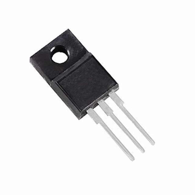
STFU6N65 N-Channel 650V 4A MOSFET Equivalent & Substitute Parts
Part Overview
The STFU6N65 is an N-Channel MOSFET rated for 650V drain-to-source voltage with 4A continuous drain current in a Through Hole TO-220FP package. This device is classified as obsolete, making identification of equivalent and substitute parts necessary for ongoing design support and procurement continuity. The STFU6N65 operates across a temperature range of -55°C to 150°C and is RoHS3 compliant with unlimited moisture sensitivity level (MSL 1).
Substiute Parts
Key Parameters
| Parameter | Value | Unit |
|---|---|---|
| Drain to Source Voltage (Vdss) | 650 | V |
| Continuous Drain Current (Id) @ 25°C | 4 | A |
| Drive Voltage (Max Rds On) | 10 | V |
| Rds On (Max) @ 2A, 10V | 2.7 | Ohm |
| Gate Threshold Voltage (Vgs(th)) @ 250µA | 4 | V |
| Maximum Gate Voltage (Vgs) | ±30 | V |
| Input Capacitance (Ciss) @ 25V | 463 | pF |
| Power Dissipation (Max) @ Ta | 620 | mW |
| Power Dissipation (Max) @ Tc | 77 | W |
| Operating Temperature Range | -55 to 150 | °C |
| Package Type | TO-220FP | Through Hole |
| Product Status | Obsolete | - |
Substitute Part Grouping Explanation
Substitution of the STFU6N65 is based on electrical and mechanical parameter compatibility within the N-Channel MOSFET category. The primary substitution criteria are:
Electrical Compatibility Parameters:
- Drain to Source Voltage (Vdss): Must equal or exceed 650V
- Continuous Drain Current (Id): Must equal or exceed 4A at 25°C
- Gate Threshold Voltage (Vgs(th)): Must be compatible at specified test conditions
- Maximum Gate Voltage (Vgs): Must accommodate ±30V or greater
- Drive Voltage: Must operate at 10V gate drive
Mechanical Compatibility Parameters:
- Package Type: TO-220FP Through Hole configuration
- Mounting Type: Through Hole
- Pin Configuration: TO-220-3 Full Pack
Compliance Parameters:
- RoHS3 Compliance required
- REACH Unaffected status required
- Moisture Sensitivity Level: MSL 1 (Unlimited)
The STF6N65M2 meets all electrical and mechanical compatibility requirements while offering improved performance characteristics and active product status.
Parameter Comparison
| Parameter | STFU6N65 | STF6N65M2 | Unit |
|---|---|---|---|
| Manufacturer | STMicroelectronics | STMicroelectronics | - |
| FET Type | N-Channel | N-Channel | - |
| Technology | MOSFET (Metal Oxide) | MOSFET (Metal Oxide) | - |
| Drain to Source Voltage (Vdss) | 650 | 650 | V |
| Continuous Drain Current (Id) @ 25°C | 4 | 4 | A |
| Drive Voltage (Max Rds On) | 10 | 10 | V |
| Rds On (Max) @ 2A, 10V | 2.7 | 1.35 | Ohm |
| Gate Threshold Voltage (Vgs(th)) @ 250µA | 4 | 4 | V |
| Maximum Gate Voltage (Vgs) | ±30 | ±25 | V |
| Input Capacitance (Ciss) | 463 @ 25V | 226 @ 100V | pF |
| Power Dissipation (Max) @ Tc | 77 | 20 | W |
| Operating Temperature Range | -55 to 150 | -55 to 150 | °C |
| Mounting Type | Through Hole | Through Hole | - |
| Package Type | TO-220FP | TO-220FP | - |
| Product Status | Obsolete | Active | - |
| RoHS Status | ROHS3 Compliant | ROHS3 Compliant | - |
| Moisture Sensitivity Level | 1 (Unlimited) | 1 (Unlimited) | - |
| REACH Status | REACH Unaffected | REACH Unaffected | - |
Engineering Selection Recommendations
Primary Substitute: STF6N65M2
The STF6N65M2 is the direct substitute for the obsolete STFU6N65. Both devices share identical electrical ratings for Vdss (650V) and Id (4A), ensuring functional compatibility in existing circuit designs. The STF6N65M2 maintains the same TO-220FP Through Hole package configuration and pin assignment, enabling direct board-level replacement without layout modifications.
Compliance and Status Advantages:
The STF6N65M2 holds Active product status, ensuring long-term availability and manufacturing support compared to the Obsolete STFU6N65. Both devices maintain RoHS3 compliance, REACH Unaffected status, and MSL 1 (Unlimited) moisture sensitivity level, satisfying regulatory and supply chain requirements.
Performance Improvements:
The STF6N65M2 incorporates MDmesh™ technology, delivering superior on-resistance characteristics (1.35Ohm vs. 2.7Ohm at 2A, 10V gate drive). This reduction in Rds On results in lower conduction losses and reduced thermal dissipation requirements. The STF6N65M2 also exhibits lower input capacitance (226pF vs. 463pF), improving switching performance and gate drive efficiency.
Thermal Considerations:
The STF6N65M2 demonstrates improved thermal performance with maximum power dissipation of 20W at Tc, compared to 77W for the STFU6N65. This enhanced thermal efficiency supports applications with stringent thermal management constraints.
Frequently Asked Questions (FAQ)
Q: Can the STF6N65M2 directly replace the STFU6N65 in existing designs?
A: Yes. The STF6N65M2 is electrically and mechanically compatible with the STFU6N65. Both devices feature identical Vdss (650V), Id (4A), Vgs(th) (4V @ 250µA), and TO-220FP package configuration. No circuit modifications or board redesign are required for direct substitution.
Q: What are the key differences between these two devices?
A: The primary differences are product status and performance characteristics. The STFU6N65 is obsolete, while the STF6N65M2 is active. The STF6N65M2 offers lower on-resistance (1.35Ohm vs. 2.7Ohm), reduced input capacitance (226pF vs. 463pF), and improved thermal performance (20W vs. 77W maximum power dissipation at Tc). The STF6N65M2 incorporates MDmesh™ technology for enhanced efficiency.
Q: Are there any gate voltage compatibility concerns?
A: The STFU6N65 supports ±30V maximum gate voltage, while the STF6N65M2 supports ±25V. For applications operating within ±25V gate drive, full compatibility is maintained. Applications requiring gate voltages between ±25V and ±30V must be evaluated against the STF6N65M2 specifications.
Q: Do both devices meet the same regulatory and compliance standards?
A: Yes. Both the STFU6N65 and STF6N65M2 are RoHS3 compliant, REACH Unaffected, and classified as MSL 1 (Unlimited) for moisture sensitivity. Both devices carry EAR99 ECCN classification and 8541.29.0095 HTSUS code.
Q: What is the impact of lower on-resistance in the STF6N65M2?
A: Lower on-resistance (1.35Ohm vs. 2.7Ohm) reduces conduction losses during device operation, resulting in lower heat generation and improved overall circuit efficiency. This characteristic is particularly beneficial in high-frequency switching applications and designs with thermal constraints.
Q: Are there any switching performance differences?
A: The STF6N65M2 exhibits lower input capacitance (226pF vs. 463pF), which reduces gate charge requirements and improves switching speed. This results in faster switching transitions and reduced gate drive power consumption compared to the STFU6N65.
Q: Is the TO-220FP package identical for both devices?
A: Yes. Both devices use the TO-220FP Through Hole package with TO-220-3 Full Pack configuration. Pin assignments and mechanical dimensions are identical, enabling direct board-level replacement without PCB modifications.
Alternative Parts

SJ6012L2TP
Littelfuse Inc.
6 Alternative Parts

JMK107BBJ476MA-RE
Taiyo Yuden
10 Alternative Parts

GMK107BBJ475MA-T
Taiyo Yuden
5 Alternative Parts
SJ6020N2ARP
Littelfuse Inc.
3 Alternative Parts
SJ6025R2ATP
Littelfuse Inc.
4 Alternative Parts

2474-05L
API Delevan Inc.
1 Alternative Parts

4590R-684K
API Delevan Inc.
1 Alternative Parts

CM6560R-334
API Delevan Inc.
1 Alternative Parts

CM6460-104
API Delevan Inc.
1 Alternative Parts

5526-12
API Delevan Inc.
1 Alternative Parts