


Request Quote
(Ships tomorrow)
STF9NK90Z Equivalent & Substitute Parts
Part Overview
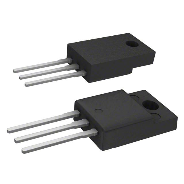
The STF9NK90Z is an N-channel 900 V MOSFET manufactured by STMicroelectronics, designed for high-voltage switching applications. This device features the SuperMESH™ technology platform and is rated for 8 A continuous drain current with a maximum power dissipation of 40 W. The part is housed in a TO-220FP through-hole package and maintains active product status with full RoHS3 compliance.
Equivalent and substitute parts are identified when alternative components meet the same electrical and mechanical specifications, enabling design flexibility, inventory optimization, and supply chain continuity for applications requiring 900 V N-channel MOSFETs in TO-220 packaging.
Substiute Parts
Key Parameters
| Parameter | Value | Unit |
|---|---|---|
| Drain to Source Voltage (Vdss) | 900 | V |
| Continuous Drain Current (Id) @ 25°C | 8 | A (Tc) |
| On-State Resistance (Rds On Max) @ 10V | 1.3 | Ohm @ 3.6A, 10V |
| Gate Threshold Voltage (Vgs th Max) | 4.5 | V @ 100µA |
| Gate Charge (Qg Max) @ 10V | 72 | nC |
| Maximum Gate Voltage (Vgs Max) | ±30 | V |
| Input Capacitance (Ciss Max) @ 25V | 2115 | pF |
| Power Dissipation (Max) | 40 | W (Tc) |
| Operating Temperature Range | -55 to 150 | °C (TJ) |
| Mounting Type | Through Hole | — |
| Package Type | TO-220-3 Full Pack | — |
| FET Type | N-Channel | — |
| Technology | MOSFET (Metal Oxide) | — |
Substitute Part Grouping Explanation
Substitution of the STF9NK90Z is determined by strict equivalence across critical electrical and mechanical parameters. The primary substitution criteria are:
Voltage Rating Equivalence: Both the main part and substitute must maintain a Drain to Source Voltage (Vdss) of 900 V to ensure compatibility in high-voltage switching circuits.
Package Compatibility: The TO-220-3 Full Pack through-hole mounting configuration is mandatory for mechanical and thermal interface compatibility with existing PCB designs and heat sink assemblies.
FET Type and Technology: N-channel MOSFET (Metal Oxide) technology is required to maintain functional equivalence in circuit topology and gate drive requirements.
Operating Temperature Range: The -55°C to 150°C (TJ) operating range must be supported to ensure reliability across specified environmental conditions.
Gate Voltage Specification: Maximum gate voltage (Vgs Max) of ±30 V ensures compatibility with standard gate drive circuits and protection schemes.
The FQPF8N90C from Fairchild Semiconductor meets these core substitution criteria, enabling direct functional replacement in applications where the specified electrical characteristics are satisfied.
Parameter Comparison
| Parameter | STF9NK90Z (STMicroelectronics) | FQPF8N90C (Fairchild Semiconductor) | Unit |
|---|---|---|---|
| Drain to Source Voltage (Vdss) | 900 | 900 | V |
| Continuous Drain Current (Id) @ 25°C | 8 | 6.3 | A (Tc) |
| On-State Resistance (Rds On Max) @ 10V | 1.3 @ 3.6A | 1.9 @ 3.15A | Ohm |
| Gate Threshold Voltage (Vgs th Max) | 4.5 @ 100µA | 5 @ 250µA | V |
| Gate Charge (Qg Max) @ 10V | 72 | 45 | nC |
| Maximum Gate Voltage (Vgs Max) | ±30 | ±30 | V |
| Input Capacitance (Ciss Max) @ 25V | 2115 | 2080 | pF |
| Power Dissipation (Max) | 40 | 60 | W (Tc) |
| Operating Temperature Range | -55 to 150 | -55 to 150 | °C (TJ) |
| Mounting Type | Through Hole | Through Hole | — |
| Package Type | TO-220-3 Full Pack | TO-220-3 Full Pack | — |
| FET Type | N-Channel | N-Channel | — |
| Technology | MOSFET (Metal Oxide) | MOSFET (Metal Oxide) | — |
Engineering Selection Recommendations
Primary Selection (STF9NK90Z): The STF9NK90Z is the specified component for applications requiring the exact electrical characteristics defined in the design. This part maintains active product status with confirmed inventory availability (4408 pcs) and full RoHS3 compliance. The SuperMESH™ technology platform provides optimized performance for the specified 8 A continuous drain current rating.
Substitute Selection (FQPF8N90C): The FQPF8N90C serves as a functional substitute when the STF9NK90Z is unavailable or when design requirements permit operation within its electrical envelope. This part is also active with higher inventory availability (24077 pcs) and maintains RoHS3 compliance through the QFET® technology platform. The FQPF8N90C exhibits lower gate charge (45 nC vs. 72 nC), which may reduce gate drive power requirements in high-frequency switching applications.
Electrical Trade-offs: The FQPF8N90C operates at a reduced continuous drain current rating (6.3 A vs. 8 A) and exhibits higher on-state resistance (1.9 Ohm vs. 1.3 Ohm). These characteristics require verification against application current demands and thermal dissipation budgets. The FQPF8N90C provides higher maximum power dissipation (60 W vs. 40 W), which may offset the higher on-state resistance in certain thermal management scenarios.
Compliance and Certification: Both parts maintain identical operating temperature ranges (-55°C to 150°C) and maximum gate voltage specifications (±30 V), ensuring compatibility with standard gate drive and protection circuits. Both parts carry EAR99 export classification and are RoHS3 compliant.
Frequently Asked Questions (FAQ)
Q: Can the FQPF8N90C directly replace the STF9NK90Z in all applications?
A: Direct replacement is possible only when the application current demand does not exceed 6.3 A continuous drain current and thermal dissipation requirements are within the FQPF8N90C's 60 W maximum rating. The higher on-state resistance (1.9 Ohm vs. 1.3 Ohm) will result in increased power dissipation at equivalent current levels. Circuit analysis is required to confirm compatibility.
Q: Are the TO-220FP and TO-220F packages mechanically interchangeable?
A: Both packages are TO-220-3 Full Pack configurations with through-hole mounting. The mechanical footprint and thermal interface are compatible for PCB assembly and heat sink mounting. The "FP" and "F" designations indicate manufacturer-specific package variants that are functionally equivalent for through-hole applications.
Q: What is the significance of the gate charge difference between these parts?
A: The STF9NK90Z exhibits 72 nC gate charge compared to 45 nC for the FQPF8N90C. Higher gate charge requires greater gate drive energy and may increase switching losses in high-frequency applications. The FQPF8N90C's lower gate charge can reduce gate driver power consumption and heat generation.
Q: Do both parts support the same gate voltage range?
A: Yes. Both the STF9NK90Z and FQPF8N90C support a maximum gate voltage (Vgs Max) of ±30 V, ensuring compatibility with standard gate drive circuits and protection schemes. Gate threshold voltages differ slightly (4.5 V vs. 5 V), which is within typical gate drive circuit tolerance.
Q: What are the inventory implications of selecting the FQPF8N90C as a substitute?
A: The FQPF8N90C maintains significantly higher inventory availability (24077 pcs vs. 4408 pcs for the STF9NK90Z). This availability advantage may support supply chain continuity and reduce lead times in applications where the electrical characteristics of the FQPF8N90C satisfy design requirements.
Q: Are there differences in the input capacitance between these parts?
A: Input capacitance (Ciss) is nearly identical: 2115 pF for the STF9NK90Z and 2080 pF for the FQPF8N90C. This minimal difference has negligible impact on gate drive circuit design and switching performance.
Q: How do the on-state resistance specifications affect thermal design?
A: The STF9NK90Z exhibits lower on-state resistance (1.3 Ohm @ 3.6A, 10V) compared to the FQPF8N90C (1.9 Ohm @ 3.15A, 10V). At equivalent current levels, the higher resistance of the FQPF8N90C generates proportionally greater heat dissipation. Thermal analysis must confirm that the FQPF8N90C's 60 W maximum power dissipation accommodates the application's duty cycle and ambient temperature conditions.
Alternative Parts

SJ6012L2TP
Littelfuse Inc.
6 Alternative Parts

JMK107BBJ476MA-RE
Taiyo Yuden
10 Alternative Parts

GMK107BBJ475MA-T
Taiyo Yuden
5 Alternative Parts
SJ6020N2ARP
Littelfuse Inc.
3 Alternative Parts
SJ6025R2ATP
Littelfuse Inc.
4 Alternative Parts

2474-05L
API Delevan Inc.
1 Alternative Parts

4590R-684K
API Delevan Inc.
1 Alternative Parts

CM6560R-334
API Delevan Inc.
1 Alternative Parts

CM6460-104
API Delevan Inc.
1 Alternative Parts

5526-12
API Delevan Inc.
1 Alternative Parts