


Request Quote
(Ships tomorrow)
STF7N52K3 Equivalent & Substitute Parts
Part Overview
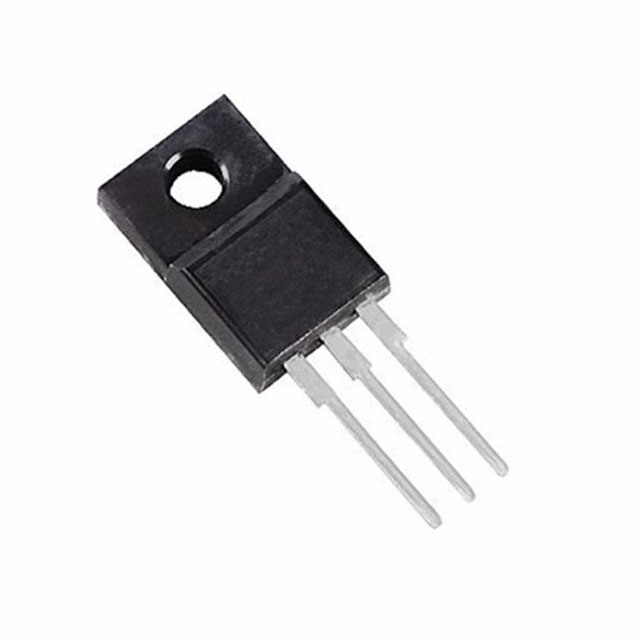
The STF7N52K3 is an N-Channel MOSFET manufactured by STMicroelectronics, rated for 525V drain-to-source voltage with 6A continuous drain current at 25°C. This device is packaged in a TO-220FP through-hole configuration and is part of the SuperMESH3™ series. The part is currently listed as obsolete, making identification of equivalent and substitute components necessary for ongoing design support, maintenance, and production continuity. Substitute parts must maintain electrical compatibility across voltage, current, and thermal specifications while accommodating packaging and mounting requirements.
Substiute Parts
Key Parameters
| Parameter | Value | Unit |
|---|---|---|
| FET Type | N-Channel | — |
| Drain to Source Voltage (Vdss) | 525 | V |
| Continuous Drain Current (Id) @ 25°C | 6 | A |
| Rds On (Max) @ Id, Vgs | 850 mOhm @ 3A, 10V | — |
| Gate Threshold Voltage (Vgs(th)) @ Id | 4.5 | V @ 50µA |
| Power Dissipation (Max) | 25 | W |
| Operating Temperature (TJ) | 150 | °C |
| Mounting Type | Through Hole | — |
| Package / Case | TO-220-3 Full Pack | — |
| RoHS Status | ROHS3 Compliant | — |
Substitute Part Grouping Explanation
Substitution of the STF7N52K3 is determined by strict alignment of electrical and mechanical parameters. The primary substitution criteria are:
Electrical Compatibility Requirements:
- FET Type: N-Channel topology must be maintained
- Drain to Source Voltage (Vdss): Substitute must equal or exceed 525V
- Continuous Drain Current (Id): Substitute must support minimum 6A at 25°C
- On-State Resistance (Rds On): Substitute must not exceed the original specification to maintain thermal performance
- Gate Threshold Voltage (Vgs(th)): Must fall within compatible operating range
- Power Dissipation: Substitute must support minimum 25W thermal rating
Mechanical Compatibility Requirements:
- Mounting Type: Through Hole configuration required
- Package / Case: TO-220-3 Full Pack or equivalent footprint compatibility
- Pin configuration: Standard three-pin MOSFET layout
Compliance Requirements:
- RoHS3 Compliance mandatory
- ECCN and HTSUS classifications must align
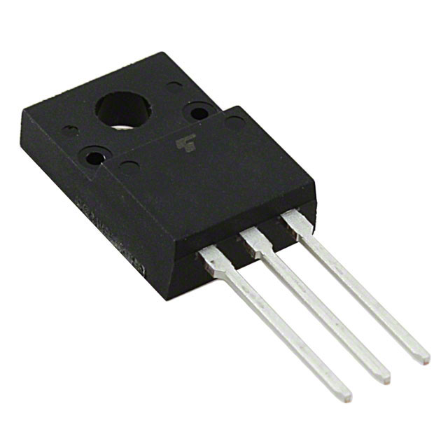
The TK10A55D(STA4,Q,M) from Toshiba Semiconductor and Storage meets these criteria with enhanced electrical performance characteristics.
Parameter Comparison
| Parameter | STF7N52K3 (STMicroelectronics) | TK10A55D(STA4,Q,M) (Toshiba) | Unit |
|---|---|---|---|
| FET Type | N-Channel | N-Channel | — |
| Drain to Source Voltage (Vdss) | 525 | 550 | V |
| Continuous Drain Current (Id) @ 25°C | 6 (Tc) | 10 (Ta) | A |
| Drive Voltage (Max Rds On) | 10 | 10 | V |
| Rds On (Max) @ Id, Vgs | 850 mOhm @ 3A, 10V | 720 mOhm @ 5A, 10V | — |
| Gate Threshold Voltage (Vgs(th)) @ Id | 4.5 @ 50µA | 4.0 @ 1mA | V |
| Gate Charge (Qg) (Max) @ Vgs | 33 @ 10V | 24 @ 10V | nC |
| Vgs (Max) | ±30 | ±30 | V |
| Power Dissipation (Max) | 25 (Tc) | 45 (Tc) | W |
| Operating Temperature (TJ) | 150 | 150 | °C |
| Mounting Type | Through Hole | Through Hole | — |
| Package / Case | TO-220-3 Full Pack | TO-220-3 Full Pack | — |
| RoHS Status | ROHS3 Compliant | ROHS3 Compliant | — |
| Product Status | Obsolete | Active | — |
Engineering Selection Recommendations
The TK10A55D(STA4,Q,M) is a direct substitute for the STF7N52K3 based on the following engineering criteria:
Electrical Performance: The substitute part exceeds the original specification in drain-to-source voltage (550V vs. 525V), continuous drain current (10A vs. 6A), and power dissipation capability (45W vs. 25W). On-state resistance is improved (720 mOhm vs. 850 mOhm), resulting in lower conduction losses. Gate charge is reduced (24 nC vs. 33 nC), enabling faster switching characteristics.
Compliance and Availability: Both parts maintain ROHS3 compliance and identical ECCN/HTSUS classifications. The substitute part carries Active product status, ensuring long-term availability and supply chain continuity, whereas the original STF7N52K3 is obsolete.
Mechanical Compatibility: Both devices utilize identical TO-220-3 Full Pack through-hole packaging, permitting direct PCB footprint compatibility without layout modifications.
Thermal and Operational Alignment: Maximum junction temperature ratings are identical at 150°C. The substitute's enhanced power dissipation capability provides thermal margin for existing designs.
Frequently Asked Questions (FAQ)
Q: Can the TK10A55D(STA4,Q,M) be used as a direct replacement for the STF7N52K3 without PCB modifications?
A: Yes. Both devices share identical TO-220-3 Full Pack through-hole packaging and pin configuration. No PCB layout changes are required for mechanical installation.
Q: What are the key electrical differences between these parts?
A: The TK10A55D(STA4,Q,M) provides higher voltage rating (550V vs. 525V), higher current capability (10A vs. 6A), lower on-state resistance (720 mOhm vs. 850 mOhm), and greater power dissipation capacity (45W vs. 25W). These represent performance enhancements over the original specification.
Q: Are both parts RoHS compliant?
A: Yes. Both the STF7N52K3 and TK10A55D(STA4,Q,M) are ROHS3 compliant and carry identical ECCN and HTSUS classifications.
Q: Why is the STF7N52K3 listed as obsolete?
A: The STF7N52K3 has reached end-of-life status with STMicroelectronics. The TK10A55D(STA4,Q,M) maintains active product status, ensuring continued availability and manufacturing support.
Q: Will the substitute part affect circuit performance?
A: The substitute part's enhanced electrical specifications (lower Rds On, reduced gate charge, higher current rating) will maintain or improve circuit performance. No adverse effects are expected in applications designed for the original part.
Q: What is the difference between the TO-220FP and TO-220SIS package designations?
A: Both designations refer to TO-220-3 Full Pack through-hole configurations with identical pin spacing and mechanical footprints. The different suffixes indicate manufacturer-specific package variants that are mechanically and electrically interchangeable.
Q: Are gate threshold voltages compatible between these parts?
A: Yes. The gate threshold voltages are compatible (4.5V vs. 4.0V at different measurement currents). Both fall within the ±30V maximum gate-source voltage specification and operate within standard MOSFET gate drive voltage ranges.
Alternative Parts

SJ6012L2TP
Littelfuse Inc.
6 Alternative Parts

JMK107BBJ476MA-RE
Taiyo Yuden
10 Alternative Parts

GMK107BBJ475MA-T
Taiyo Yuden
5 Alternative Parts
SJ6020N2ARP
Littelfuse Inc.
3 Alternative Parts
SJ6025R2ATP
Littelfuse Inc.
4 Alternative Parts

2474-05L
API Delevan Inc.
1 Alternative Parts

4590R-684K
API Delevan Inc.
1 Alternative Parts

CM6560R-334
API Delevan Inc.
1 Alternative Parts

CM6460-104
API Delevan Inc.
1 Alternative Parts

5526-12
API Delevan Inc.
1 Alternative Parts