


Request Quote
(Ships tomorrow)
STD7N60DM2 Equivalent & Substitute Parts
Part Overview
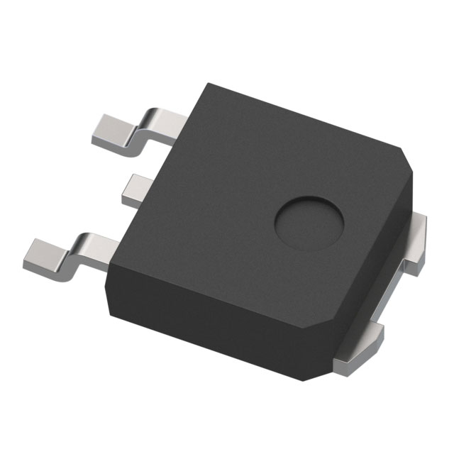
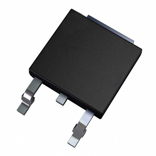
The STD7N60DM2 is an N-Channel 600V 6A MOSFET manufactured by STMicroelectronics in the MDmesh™ DM2 series. This device is packaged in TO-252 (DPAK) surface mount configuration and is rated for 60W power dissipation. The part is currently Active in product status with 2495 units in stock.
Equivalent and substitute parts are necessary when the primary part becomes unavailable, when alternative sourcing is required for supply chain resilience, or when design flexibility permits selection from multiple qualified manufacturers offering comparable electrical and mechanical characteristics within the same voltage and current ratings.
Substiute Parts
Key Parameters
| Parameter | Value | Unit |
|---|---|---|
| Drain to Source Voltage (Vdss) | 600 | V |
| Continuous Drain Current (Id) @ 25°C | 6 | A |
| Power Dissipation (Max) | 60 | W |
| Rds On (Max) @ Id, Vgs | 900 mOhm @ 3A, 10V | Ω |
| Gate Charge (Qg) (Max) @ Vgs | 7.5 | nC @ 10V |
| Operating Temperature Range | -55 to 150 | °C |
| Mounting Type | Surface Mount | TO-252 (DPAK) |
| RoHS Status | ROHS3 Compliant | — |
Substitute Part Grouping Explanation
Substitution eligibility for the STD7N60DM2 is determined by the following critical parameters:
Primary Substitution Criteria:
- Drain to Source Voltage (Vdss): 600V (exact match required)
- Mounting Type: Surface Mount TO-252 (DPAK) package family
- FET Type: N-Channel MOSFET
- Operating Temperature Range: Minimum -55°C to 150°C
Secondary Compatibility Parameters:
- Continuous Drain Current (Id): 6A or greater
- Power Dissipation: 60W or greater
- Gate Charge (Qg): Lower values preferred for switching efficiency
- Rds On: Lower values preferred for reduced conduction losses
Parts are grouped into two categories based on substitution suitability:
Category A - Direct Substitutes (Preferred): Parts meeting all primary criteria with Id ≥ 6A and power dissipation ≥ 60W, maintaining Active product status.
Category B - Functional Equivalents (Alternative): Parts meeting all primary criteria with Id ≥ 5.4A and power dissipation ≥ 54W, including parts with Not For New Designs or Last Time Buy status.
Parameter Comparison
| Parameter | STD7N60DM2 (Main) | TK5P60W,RVQ | FCD5N60TM-WS | FCD4N60TM | R6006ANDTL | R6007RND3TL1 |
|---|---|---|---|---|---|---|
| Manufacturer | STMicroelectronics | Toshiba | onsemi | onsemi | Rohm Semiconductor | Rohm Semiconductor |
| Vdss (V) | 600 | 600 | 600 | 600 | 600 | 600 |
| Id @ 25°C (A) | 6 | 5.4 | 4.6 | 3.9 | 6 | 7 |
| Power Dissipation (W) | 60 | 60 | 54 | 50 | 40 | 96 |
| Rds On (Max) @ Vgs 10V (mOhm) | 900 @ 3A | 900 @ 2.7A | 950 @ 2.3A | 1200 @ 2A | 1200 @ 3A | 940 @ 3.5A, 15V |
| Gate Charge Qg (nC) | 7.5 @ 10V | 10.5 @ 10V | 16 @ 10V | 16.6 @ 10V | 15 @ 10V | 17.5 @ 15V |
| Operating Temperature (°C) | -55 to 150 | -55 to 150 | -55 to 150 | -55 to 150 | -55 to 150 | -55 to 150 |
| Package | TO-252 (DPAK) | TO-252 (DPAK) | TO-252AA (DPAK) | TO-252AA (DPAK) | CPT3 | TO-252 (DPAK) |
| Product Status | Active | Active | Not For New Designs | Not For New Designs | Last Time Buy | Active |
| RoHS Status | ROHS3 Compliant | ROHS3 Compliant | ROHS3 Compliant | ROHS3 Compliant | ROHS3 Compliant | ROHS3 Compliant |
Engineering Selection Recommendations
Recommended Primary Substitute: TK5P60W,RVQ (Toshiba)
The TK5P60W,RVQ meets all primary substitution criteria with Active product status. It provides 5.4A continuous drain current and 60W power dissipation, matching the thermal envelope of the STD7N60DM2. Gate charge of 10.5 nC is slightly elevated compared to the main part but remains within acceptable switching efficiency parameters. This part is suitable for direct replacement in new designs and ongoing production.
Recommended Secondary Substitute: R6007RND3TL1 (Rohm Semiconductor)
The R6007RND3TL1 offers superior current handling at 7A continuous drain current and 96W power dissipation, providing design margin for applications requiring higher current capacity. Active product status and full compliance certifications support its use in new designs. The higher gate charge (17.5 nC) and drive voltage requirement (15V) must be verified against gate driver capabilities in the target application.
Alternative Substitutes with Limitations:
FCD5N60TM-WS (onsemi) and FCD4N60TM (onsemi) are functionally equivalent but carry Not For New Designs status. These parts are suitable only for sustaining production of existing designs or as temporary solutions during supply constraints. Current ratings of 4.6A and 3.9A respectively are below the main part specification and may require thermal derating in high-current applications.
R6006ANDTL (Rohm Semiconductor) carries Last Time Buy status and is not recommended for new designs. Power dissipation of 40W is below the main part specification and may introduce thermal limitations.
Compliance and Certification:
All substitute parts maintain ROHS3 compliance and REACH Unaffected status, matching the environmental and regulatory posture of the STD7N60DM2. All parts are classified under ECCN EAR99 and HTSUS 8541.29.0095.
Frequently Asked Questions (FAQ)
Q: Can the TK5P60W,RVQ be used as a direct replacement for the STD7N60DM2 in existing designs?
A: Yes. The TK5P60W,RVQ maintains identical voltage rating (600V), comparable current rating (5.4A vs. 6A), matching power dissipation (60W), and identical package (TO-252 DPAK). Operating temperature range and compliance certifications are equivalent. Gate charge is slightly higher (10.5 nC vs. 7.5 nC), which may increase switching losses marginally but remains within typical design tolerances.
Q: What is the difference between TO-252 (DPAK) and TO-252AA (DPAK) packages?
A: Both designations refer to the same physical TO-252 surface mount package with three leads (two signal leads plus tab). The "AA" suffix in TO-252AA indicates a specific variant designation used by onsemi. Pin compatibility and PCB footprint are identical. No layout or assembly changes are required when substituting between these package variants.
Q: Why do some substitute parts show "Not For New Designs" status?
A: Parts marked "Not For New Designs" are in mature or declining production phases. Manufacturers apply this status when transitioning products to end-of-life or when newer alternatives are available. These parts remain available for sustaining production of existing designs but should not be selected for new product development due to potential future availability constraints.
Q: Is the R6007RND3TL1 suitable for applications requiring exactly 6A continuous current?
A: Yes. The R6007RND3TL1 provides 7A continuous drain current, which exceeds the 6A requirement of the STD7N60DM2. This provides design margin and thermal headroom. However, the higher gate charge (17.5 nC) and increased drive voltage requirement (15V) must be verified against the gate driver circuit specifications to ensure proper switching performance.
Q: What thermal considerations apply when substituting parts with different power dissipation ratings?
A: Power dissipation ratings reflect maximum thermal capability under specified conditions. The STD7N60DM2 is rated for 60W. Substitutes with lower ratings (FCD4N60TM at 50W, R6006ANDTL at 40W) may require thermal derating in high-power applications. Substitutes with higher ratings (R6007RND3TL1 at 96W) provide additional thermal margin. PCB thermal design, heatsinking, and ambient temperature must be evaluated for each application.
Q: Are all substitute parts RoHS3 compliant?
A: Yes. All substitute parts listed carry ROHS3 Compliant status, matching the environmental compliance of the STD7N60DM2. All parts are also REACH Unaffected, indicating no restricted substances of concern.
Q: What is the significance of gate charge (Qg) differences between parts?
A: Gate charge determines the energy required to switch the MOSFET on and off. Lower gate charge (STD7N60DM2 at 7.5 nC) reduces switching losses and allows faster switching speeds with lower gate driver power consumption. Higher gate charge in substitute parts (up to 17.5 nC in R6007RND3TL1) increases switching losses and may require higher gate driver current capability. Gate driver circuit design must accommodate the gate charge specification of the selected part.
Q: Can parts with different Rds On values be substituted without circuit modification?
A: Rds On (on-state resistance) directly affects conduction losses and heat generation. Lower Rds On values reduce losses and improve efficiency. The STD7N60DM2 specifies 900 mOhm at 3A, 10V. Substitutes with higher Rds On values (up to 1200 mOhm) will increase conduction losses proportionally. Thermal design and efficiency calculations must be re-evaluated when substituting parts with significantly different Rds On specifications. Higher Rds On parts may require enhanced heatsinking or thermal management.
Alternative Parts

SJ6012L2TP
Littelfuse Inc.
6 Alternative Parts

JMK107BBJ476MA-RE
Taiyo Yuden
10 Alternative Parts

GMK107BBJ475MA-T
Taiyo Yuden
5 Alternative Parts
SJ6020N2ARP
Littelfuse Inc.
3 Alternative Parts
SJ6025R2ATP
Littelfuse Inc.
4 Alternative Parts

2474-05L
API Delevan Inc.
1 Alternative Parts

4590R-684K
API Delevan Inc.
1 Alternative Parts

CM6560R-334
API Delevan Inc.
1 Alternative Parts

CM6460-104
API Delevan Inc.
1 Alternative Parts

5526-12
API Delevan Inc.
1 Alternative Parts