


Request Quote
(Ships tomorrow)
STB24N65M2 Equivalent & Substitute Parts
Part Overview
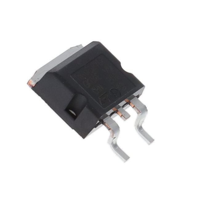
The STB24N65M2 is an N-Channel 650V 16A MOSFET manufactured by STMicroelectronics, housed in a D2PAK surface mount package. This device belongs to the MDmesh™ M2 series and is designed for high-voltage switching applications requiring continuous drain current capability at elevated temperatures.
The STB24N65M2 carries an Obsolete product status. Locating equivalent or substitute components becomes necessary when original inventory is depleted or when design flexibility is required for long-term production planning. Substitute parts must maintain compatibility across critical electrical parameters including drain-source voltage rating, continuous drain current, on-state resistance, and thermal characteristics, while accommodating the D2PAK package form factor.
Substiute Parts
Key Parameters
| Parameter | Value | Unit |
|---|---|---|
| Drain to Source Voltage (Vdss) | 650 | V |
| Current - Continuous Drain (Id) @ 25°C | 16 | A (Tc) |
| Rds On (Max) @ Id, Vgs | 230 | mOhm @ 8A, 10V |
| Gate Charge (Qg) (Max) @ Vgs | 29 | nC @ 10V |
| Power Dissipation (Max) | 150 | W (Tc) |
| Operating Temperature Range | -55 to 150 | °C (TJ) |
| Package Type | D2PAK (TO-263-3) | Surface Mount |
| Vgs(th) (Max) @ Id | 4 | V @ 250µA |
| Input Capacitance (Ciss) (Max) @ Vds | 1060 | pF @ 100V |
Substitute Part Grouping Explanation
Substitution eligibility for the STB24N65M2 is determined by strict alignment with the following critical electrical and mechanical parameters:
Voltage Rating Requirement: The substitute must maintain a Drain to Source Voltage (Vdss) rating of 650V to ensure equivalent circuit protection and voltage withstand capability.
Current Capacity Requirement: The substitute must support a continuous drain current (Id) rating that meets or exceeds 16A at 25°C to maintain thermal and electrical performance margins in the application.
On-State Resistance (Rds On): The substitute must demonstrate an Rds On specification that does not exceed the maximum specified value to prevent excessive power dissipation and thermal runaway conditions.
Package Compatibility Requirement: The substitute must utilize the D2PAK (TO-263-3) surface mount package to ensure mechanical and thermal interface compatibility with existing PCB layouts and thermal management systems.
Temperature Operating Range: The substitute must support the full operating temperature range of -55°C to 150°C (TJ) to maintain functional reliability across all specified environmental conditions.
Gate Charge and Input Capacitance: These parameters influence switching speed and driver circuit design; substitutes must remain within acceptable ranges to prevent circuit performance degradation.
The FCB260N65S3 from onsemi is identified as a substitute part. While this device maintains the 650V voltage rating and D2PAK package compatibility, it exhibits a reduced continuous drain current rating of 12A and lower power dissipation of 90W compared to the STB24N65M2. This substitution is valid only for applications where the 12A current capacity and 90W thermal budget are sufficient for the intended circuit operation.
Parameter Comparison
| Parameter | STB24N65M2 (Main) | FCB260N65S3 (Substitute) | Unit |
|---|---|---|---|
| Manufacturer | STMicroelectronics | onsemi | — |
| Drain to Source Voltage (Vdss) | 650 | 650 | V |
| Current - Continuous Drain (Id) @ 25°C | 16 | 12 | A (Tc) |
| Rds On (Max) @ Id, Vgs | 230 @ 8A, 10V | 260 @ 6A, 10V | mOhm |
| Gate Charge (Qg) (Max) @ Vgs | 29 | 24 | nC @ 10V |
| Power Dissipation (Max) | 150 | 90 | W (Tc) |
| Operating Temperature Range | -55 to 150 | -55 to 150 | °C (TJ) |
| Package Type | D2PAK (TO-263-3) | D2PAK (TO-263-3) | Surface Mount |
| Vgs(th) (Max) @ Id | 4 | 4.5 | V @ 250µA / 1.2mA |
| Input Capacitance (Ciss) (Max) @ Vds | 1060 @ 100V | 1010 @ 400V | pF |
| Vgs (Max) | ±25 | ±30 | V |
| Product Status | Obsolete | Not For New Designs | — |
| RoHS Status | ROHS3 Compliant | ROHS3 Compliant | — |
| Moisture Sensitivity Level (MSL) | 1 (Unlimited) | 1 (Unlimited) | — |
Engineering Selection Recommendations
STB24N65M2 (Main Part): This component carries an Obsolete product status and is no longer recommended for new designs. However, 5755 units remain in current inventory. The STB24N65M2 is suitable for sustaining existing production runs or field service applications where the original specification must be maintained. Both RoHS3 compliance and MSL Level 1 certification confirm environmental and handling compatibility with modern manufacturing processes.
FCB260N65S3 (Substitute Part): This onsemi device carries a Not For New Designs status, indicating limited long-term availability. The FCB260N65S3 maintains full voltage rating compatibility (650V) and package form factor (D2PAK) with the STB24N65M2. However, the reduced continuous drain current (12A versus 16A) and lower power dissipation rating (90W versus 150W) restrict its application scope. The FCB260N65S3 is suitable only for circuits where the 12A current capacity and 90W thermal budget satisfy the design requirements. Both components achieve RoHS3 compliance and MSL Level 1 certification.
Substitution Feasibility: Direct substitution of the FCB260N65S3 for the STB24N65M2 is valid only when circuit analysis confirms that continuous drain current does not exceed 12A and total power dissipation remains below 90W under worst-case operating conditions. The slightly higher gate threshold voltage (4.5V versus 4V) and marginally higher on-state resistance (260mOhm versus 230mOhm) introduce minor performance variations that must be evaluated within the specific application context.
Frequently Asked Questions (FAQ)
Q: Can the FCB260N65S3 directly replace the STB24N65M2 in all applications?
A: No. The FCB260N65S3 exhibits reduced current and power ratings. Direct replacement is valid only when the application circuit operates at or below 12A continuous drain current and 90W power dissipation. Applications requiring the full 16A capacity or 150W thermal capability must retain the STB24N65M2 or identify alternative 650V MOSFETs with equivalent or superior current ratings.
Q: Are the D2PAK packages physically identical between these two parts?
A: Both the STB24N65M2 and FCB260N65S3 utilize the D2PAK (TO-263-3) surface mount package with identical pinout and mechanical dimensions. PCB layout and thermal interface compatibility are maintained between these devices.
Q: What is the significance of the Obsolete and Not For New Designs product statuses?
A: The STB24N65M2 Obsolete status indicates that STMicroelectronics has discontinued production and will not accept new orders. The FCB260N65S3 Not For New Designs status indicates that onsemi discourages use in new circuit designs but may continue limited production for existing customers. Both statuses reflect end-of-life positioning and warrant consideration of alternative 650V N-Channel MOSFETs for new product development.
Q: How do the on-state resistance specifications compare between these devices?
A: The STB24N65M2 specifies 230mOhm maximum at 8A and 10V gate-source voltage. The FCB260N65S3 specifies 260mOhm maximum at 6A and 10V gate-source voltage. The FCB260N65S3 exhibits higher on-state resistance, resulting in increased power dissipation at equivalent current levels. This difference must be factored into thermal design calculations.
Q: Are both components RoHS compliant?
A: Yes. Both the STB24N65M2 and FCB260N65S3 achieve RoHS3 compliance and carry MSL Level 1 (Unlimited) moisture sensitivity ratings, confirming compatibility with lead-free soldering processes and standard storage conditions.
Q: What is the impact of the different gate threshold voltages?
A: The STB24N65M2 specifies a maximum gate threshold voltage of 4V at 250µA, while the FCB260N65S3 specifies 4.5V at 1.2mA. The higher threshold voltage of the FCB260N65S3 may require slightly higher gate drive voltage to achieve full on-state conduction. Driver circuit design must accommodate this variation to ensure reliable switching performance.
Q: Can these MOSFETs be used interchangeably in high-frequency switching applications?
A: Gate charge specifications differ slightly (29nC for STB24N65M2 versus 24nC for FCB260N65S3), influencing switching speed and driver circuit requirements. The FCB260N65S3 exhibits lower gate charge, potentially enabling faster switching transitions. However, substitution in high-frequency applications requires verification that the reduced current and power ratings do not compromise circuit performance or thermal management.
Alternative Parts

SJ6012L2TP
Littelfuse Inc.
6 Alternative Parts

JMK107BBJ476MA-RE
Taiyo Yuden
10 Alternative Parts

GMK107BBJ475MA-T
Taiyo Yuden
5 Alternative Parts
SJ6020N2ARP
Littelfuse Inc.
3 Alternative Parts
SJ6025R2ATP
Littelfuse Inc.
4 Alternative Parts

2474-05L
API Delevan Inc.
1 Alternative Parts

4590R-684K
API Delevan Inc.
1 Alternative Parts

CM6560R-334
API Delevan Inc.
1 Alternative Parts

CM6460-104
API Delevan Inc.
1 Alternative Parts

5526-12
API Delevan Inc.
1 Alternative Parts