


Request Quote
(Ships tomorrow)
SSR1N60BTM Equivalent & Substitute Parts
Part Overview
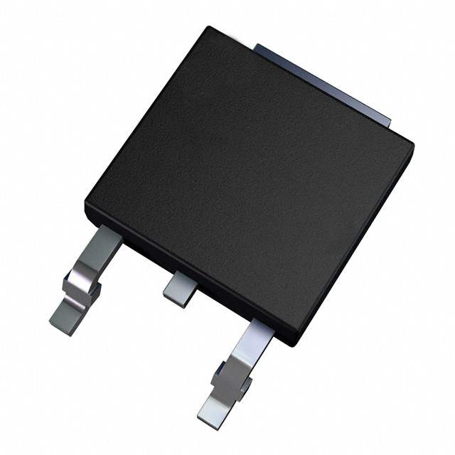
The SSR1N60BTM is an N-Channel MOSFET manufactured by onsemi, rated for 600V drain-to-source voltage with 900mA continuous drain current in a surface mount DPAK package. This device is classified as obsolete, necessitating identification of equivalent substitute components for ongoing design support and procurement continuity. The part operates across a temperature range of -55°C to 150°C and is suitable for applications requiring high-voltage switching in compact form factors.
Substiute Parts
Key Parameters
| Parameter | Value | Unit |
|---|---|---|
| Drain-to-Source Voltage (Vdss) | 600 | V |
| Continuous Drain Current (Id) @ 25°C | 900 | mA |
| On-State Resistance (Rds On) @ 450mA, 10V | 12 | Ohm |
| Gate Threshold Voltage (Vgs(th)) @ 250µA | 4 | V |
| Gate Charge (Qg) @ 10V | 7.7 | nC |
| Input Capacitance (Ciss) @ 25V | 215 | pF |
| Power Dissipation (Max) @ Tc | 28 | W |
| Operating Temperature Range | -55 to 150 | °C |
| Package Type | TO-252-3 DPAK | — |
| FET Type | N-Channel | — |
| Technology | MOSFET (Metal Oxide) | — |
Substitute Part Grouping Explanation
Substitute components for the SSR1N60BTM are identified based on strict electrical and mechanical parameter alignment within the N-Channel MOSFET category. The substitution criteria are:
Primary Matching Parameters:
- Drain-to-Source Voltage (Vdss): 600V minimum
- Package Type: TO-252-3 DPAK surface mount
- FET Type: N-Channel
- Technology: MOSFET (Metal Oxide)
- Operating Temperature Range: -55°C to 150°C minimum
Secondary Compatibility Parameters:
- Continuous Drain Current (Id): Equal to or greater than 900mA
- On-State Resistance (Rds On): Equal to or lower than 12 Ohm at specified conditions
- Gate Threshold Voltage (Vgs(th)): Within ±30V maximum gate voltage specification
- Input Capacitance (Ciss): Acceptable for switching applications
- Power Dissipation: Sufficient thermal capability for application requirements
The STD1NK60T4 from STMicroelectronics meets all primary and secondary criteria, offering improved electrical performance characteristics while maintaining package and voltage compatibility.
Parameter Comparison
| Parameter | SSR1N60BTM (onsemi) | STD1NK60T4 (STMicroelectronics) | Unit |
|---|---|---|---|
| Drain-to-Source Voltage (Vdss) | 600 | 600 | V |
| Continuous Drain Current (Id) @ 25°C | 900 | 1000 | mA |
| On-State Resistance (Rds On) @ 10V | 12 @ 450mA | 8.5 @ 500mA | Ohm |
| Gate Threshold Voltage (Vgs(th)) @ 250µA | 4 | 3.7 | V |
| Gate Charge (Qg) @ 10V | 7.7 | 10 | nC |
| Input Capacitance (Ciss) @ 25V | 215 | 156 | pF |
| Power Dissipation (Max) @ Tc | 28 | 30 | W |
| Operating Temperature Range | -55 to 150 | -55 to 150 | °C |
| Package Type | TO-252-3 DPAK | TO-252-3 DPAK | — |
| FET Type | N-Channel | N-Channel | — |
| Technology | MOSFET (Metal Oxide) | MOSFET (Metal Oxide) | — |
| Maximum Gate Voltage (Vgs) | ±30 | ±30 | V |
Engineering Selection Recommendations
The STD1NK60T4 is a direct substitute for the obsolete SSR1N60BTM based on the following engineering criteria:
Product Status Consideration: The SSR1N60BTM is classified as obsolete, while the STD1NK60T4 maintains active product status with current manufacturing support and availability. This status difference is critical for long-term supply chain reliability.
Compliance and Certification: The STD1NK60T4 carries RoHS3 compliance certification, whereas the SSR1N60BTM does not specify RoHS status. Both components are REACH Unaffected and classified under ECCN EAR99. The STD1NK60T4's RoHS3 compliance provides additional regulatory alignment for applications subject to environmental directives.
Electrical Performance: The STD1NK60T4 demonstrates superior electrical characteristics across all measured parameters. The reduced on-state resistance (8.5 Ohm versus 12 Ohm) and lower input capacitance (156 pF versus 215 pF) result in improved switching efficiency and reduced gate drive requirements. The increased continuous drain current rating (1A versus 900mA) and power dissipation capability (30W versus 28W) provide additional design margin.
Package and Thermal Compatibility: Both components utilize identical TO-252-3 DPAK surface mount packaging, ensuring mechanical and thermal interface compatibility without PCB redesign.
Moisture Sensitivity: Both components carry MSL 1 (Unlimited) classification, indicating no moisture sensitivity constraints during storage and handling.
Frequently Asked Questions (FAQ)
Q: Can the STD1NK60T4 be used as a direct replacement for the SSR1N60BTM in existing designs?
A: Yes. The STD1NK60T4 is electrically and mechanically compatible with the SSR1N60BTM. Both devices share identical drain-to-source voltage ratings (600V), package type (TO-252-3 DPAK), operating temperature range (-55°C to 150°C), and gate voltage specifications (±30V). The STD1NK60T4 provides equal or superior performance across all electrical parameters.
Q: What are the key electrical differences between these two MOSFETs?
A: The STD1NK60T4 offers improved performance in three areas: (1) On-state resistance is reduced from 12 Ohm to 8.5 Ohm, resulting in lower conduction losses; (2) Input capacitance is reduced from 215 pF to 156 pF, enabling faster switching transitions; (3) Continuous drain current is increased from 900mA to 1A, and power dissipation capability is increased from 28W to 30W, providing additional thermal headroom.
Q: Are there any package or pinout differences between these components?
A: No. Both the SSR1N60BTM and STD1NK60T4 use the TO-252-3 DPAK package with identical pinout and mechanical dimensions. No PCB layout modifications are required for substitution.
Q: What is the significance of the STD1NK60T4's RoHS3 compliance?
A: RoHS3 compliance indicates that the STD1NK60T4 meets the Restriction of Hazardous Substances Directive requirements, restricting the use of specific hazardous materials in electrical and electronic equipment. This certification is required for products sold in the European Union and is increasingly required by global manufacturers. The SSR1N60BTM does not specify RoHS status.
Q: Why is the SSR1N60BTM classified as obsolete?
A: The SSR1N60BTM is an older design that has been superseded by newer MOSFET technologies offering improved performance and compliance certifications. onsemi has discontinued active production and support for this part number. The STD1NK60T4 represents a modern equivalent with active manufacturing status.
Q: Are there any thermal management considerations when substituting these parts?
A: Both components are rated for identical operating temperature ranges (-55°C to 150°C junction temperature). The STD1NK60T4's improved on-state resistance (8.5 Ohm versus 12 Ohm) results in lower power dissipation at equivalent current levels, potentially reducing thermal management requirements. The increased power dissipation rating (30W versus 28W) provides additional thermal margin.
Q: What is the gate charge difference, and does it affect gate drive circuit design?
A: The STD1NK60T4 has a gate charge of 10 nC compared to 7.7 nC for the SSR1N60BTM. This 2.3 nC difference is negligible for most gate drive circuits. Both devices operate within the same ±30V gate voltage specification and 10V drive voltage range, requiring no gate drive circuit modifications.
Q: Are moisture sensitivity levels identical for both components?
A: Yes. Both the SSR1N60BTM and STD1NK60T4 carry MSL 1 (Unlimited) classification, indicating no moisture sensitivity constraints. Both components can be stored and handled without special moisture control measures.
Alternative Parts

SJ6012L2TP
Littelfuse Inc.
6 Alternative Parts

JMK107BBJ476MA-RE
Taiyo Yuden
10 Alternative Parts

GMK107BBJ475MA-T
Taiyo Yuden
5 Alternative Parts
SJ6020N2ARP
Littelfuse Inc.
3 Alternative Parts
SJ6025R2ATP
Littelfuse Inc.
4 Alternative Parts

2474-05L
API Delevan Inc.
1 Alternative Parts

4590R-684K
API Delevan Inc.
1 Alternative Parts

CM6560R-334
API Delevan Inc.
1 Alternative Parts

CM6460-104
API Delevan Inc.
1 Alternative Parts

5526-12
API Delevan Inc.
1 Alternative Parts