


Request Quote
(Ships tomorrow)
SPI42N03S2L-13 Equivalent & Substitute Parts
Part Overview
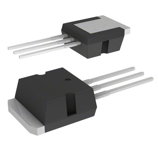
The SPI42N03S2L-13 is an N-Channel MOSFET manufactured by Infineon Technologies, rated for 30V drain-to-source voltage with a continuous drain current of 42A at 25°C. This device is housed in a TO-262-3 (I2PAK) through-hole package and is designed for power switching applications requiring moderate current handling and thermal dissipation up to 83W.
The SPI42N03S2L-13 is classified as obsolete. Locating equivalent or substitute components is necessary to support ongoing production requirements, field repairs, and system maintenance where this part number is specified in original designs.
Substiute Parts
Key Parameters
| Parameter | Value | Unit |
|---|---|---|
| Drain-to-Source Voltage (Vdss) | 30 | V |
| Continuous Drain Current (Id) @ 25°C | 42 | A |
| On-State Resistance (Rds On Max) @ Id, Vgs | 12.9 mOhm @ 21A, 10V | mOhm |
| Gate Threshold Voltage (Vgs(th) Max) @ Id | 2 | V @ 37µA |
| Power Dissipation (Max) | 83 | W |
| Operating Temperature Range | -55 to 175 | °C |
| Package Type | TO-262-3 (I2PAK) | Through Hole |
| Gate Charge (Qg Max) @ Vgs | 30.5 | nC @ 10V |
| Input Capacitance (Ciss Max) @ Vds | 1130 | pF @ 25V |
Substitute Part Grouping Explanation
Substitution of the SPI42N03S2L-13 is determined by electrical and mechanical compatibility within the following critical parameters:
Electrical Compatibility Criteria:
- Drain-to-Source Voltage (Vdss) must equal or exceed 30V
- Continuous Drain Current (Id) must meet or exceed 42A at 25°C
- On-State Resistance (Rds On) must not significantly degrade circuit performance
- Gate Threshold Voltage (Vgs(th)) must remain within acceptable drive voltage ranges
- Power Dissipation capability must support thermal requirements
- Operating Temperature Range must encompass -55°C to 175°C
Mechanical Compatibility Criteria:
- Package must be TO-262-3 (I2PAK) through-hole configuration
- Pin configuration must be identical for direct board-level substitution
- Mounting type must be through-hole
The STI55NF03L from STMicroelectronics meets these substitution criteria with equivalent voltage ratings, enhanced current capability, and compatible packaging.
Parameter Comparison
| Parameter | SPI42N03S2L-13 (Infineon) | STI55NF03L (STMicroelectronics) | Compatibility |
|---|---|---|---|
| Drain-to-Source Voltage (Vdss) | 30 V | 30 V | Equivalent |
| Continuous Drain Current (Id) @ 25°C | 42 A | 55 A | Substitute exceeds requirement |
| On-State Resistance (Rds On Max) | 12.9 mOhm @ 21A, 10V | 13 mOhm @ 27.5A, 10V | Comparable |
| Gate Threshold Voltage (Vgs(th) Max) | 2 V @ 37µA | 2.5 V @ 250µA | Compatible within drive voltage range |
| Power Dissipation (Max) | 83 W | 80 W | Substitute slightly lower; acceptable for equivalent applications |
| Operating Temperature Range | -55 to 175 °C | -60 to 175 °C | Substitute exceeds lower temperature limit |
| Package Type | TO-262-3 (I2PAK) | TO-262-3 (I2PAK) | Identical |
| Gate Charge (Qg Max) | 30.5 nC @ 10V | 27 nC @ 4.5V | Substitute lower; faster switching response |
| Input Capacitance (Ciss Max) | 1130 pF @ 25V | 1265 pF @ 25V | Comparable |
| Vgs (Max) | ±20 V | ±16 V | Substitute has lower gate voltage rating |
Engineering Selection Recommendations
Product Status Consideration: Both the SPI42N03S2L-13 and STI55NF03L are classified as obsolete. Selection between these parts should be based on current inventory availability and long-term supply chain viability.
Compliance and Certification: The STI55NF03L carries RoHS3 compliance certification, whereas the SPI42N03S2L-13 does not specify RoHS status. Both parts are REACH Unaffected and classified under ECCN EAR99. For applications requiring RoHS compliance, the STI55NF03L is the appropriate selection.
Electrical Performance: The STI55NF03L provides higher continuous drain current (55A versus 42A), enabling operation with greater design margin in current-limited applications. The lower gate charge (27 nC versus 30.5 nC) results in faster switching transitions. The on-state resistance remains comparable between both devices.
Thermal Considerations: The SPI42N03S2L-13 offers slightly higher power dissipation capability (83W versus 80W). For applications operating near thermal limits, the original part may be preferable. For most standard applications, the STI55NF03L thermal rating is sufficient.
Gate Voltage Rating: The SPI42N03S2L-13 supports ±20V gate voltage, while the STI55NF03L is rated for ±16V. Circuits designed for the full ±20V range require the original part or verification that gate drive circuits operate within ±16V limits.
Frequently Asked Questions (FAQ)
Q: Can the STI55NF03L directly replace the SPI42N03S2L-13 on a printed circuit board?
A: Yes, the STI55NF03L is a direct mechanical and electrical substitute for through-hole board-level replacement. Both devices use identical TO-262-3 (I2PAK) packaging with the same pin configuration and lead spacing. No PCB modifications are required.
Q: What are the key electrical differences between these two MOSFETs?
A: The primary differences are: (1) Continuous drain current: STI55NF03L provides 55A versus 42A for the SPI42N03S2L-13, (2) Gate charge: STI55NF03L has lower gate charge (27 nC versus 30.5 nC), enabling faster switching, (3) Maximum gate voltage: SPI42N03S2L-13 supports ±20V versus ±16V for STI55NF03L, (4) Power dissipation: SPI42N03S2L-13 rated at 83W versus 80W for STI55NF03L. Both devices maintain equivalent 30V drain-to-source voltage ratings and comparable on-state resistance.
Q: Is the STI55NF03L suitable for applications originally designed for the SPI42N03S2L-13?
A: The STI55NF03L is suitable for applications where gate drive circuits operate within ±16V limits and where the 80W power dissipation rating meets thermal requirements. The higher current rating (55A) provides additional design margin. Applications requiring the full ±20V gate voltage range or operating at maximum thermal limits (83W) should retain the original SPI42N03S2L-13 if available.
Q: What is the significance of the RoHS3 compliance on the STI55NF03L?
A: RoHS3 compliance indicates the STI55NF03L meets Restriction of Hazardous Substances Directive requirements, restricting the use of specific hazardous materials in electrical and electronic equipment. For applications subject to RoHS regulations or customer requirements, the STI55NF03L is the compliant selection. The SPI42N03S2L-13 does not specify RoHS status.
Q: Are there any circuit design considerations when substituting the STI55NF03L for the SPI42N03S2L-13?
A: Gate drive circuits must be verified to operate within the STI55NF03L's ±16V maximum gate voltage rating if the original design utilized the full ±20V range of the SPI42N03S2L-13. The lower gate charge of the STI55NF03L may result in faster switching transitions, which should be evaluated for electromagnetic compatibility and switching noise in the application. Thermal design should account for the 80W maximum power dissipation rating.
Q: What is the operating temperature range difference between these devices?
A: The SPI42N03S2L-13 operates from -55°C to 175°C, while the STI55NF03L operates from -60°C to 175°C. The STI55NF03L extends the lower temperature limit by 5°C, providing broader low-temperature operation capability. Both devices support the same upper temperature limit of 175°C.
Q: Why are both of these MOSFETs classified as obsolete?
A: Obsolete classification indicates these parts are no longer in active production by their respective manufacturers. Existing inventory from authorized distributors may remain available for a limited period. For new designs or long-term production requirements, evaluation of current-generation MOSFET alternatives with equivalent or superior specifications is recommended.
Alternative Parts

SJ6012L2TP
Littelfuse Inc.
6 Alternative Parts

JMK107BBJ476MA-RE
Taiyo Yuden
10 Alternative Parts

GMK107BBJ475MA-T
Taiyo Yuden
5 Alternative Parts
SJ6020N2ARP
Littelfuse Inc.
3 Alternative Parts
SJ6025R2ATP
Littelfuse Inc.
4 Alternative Parts

2474-05L
API Delevan Inc.
1 Alternative Parts

4590R-684K
API Delevan Inc.
1 Alternative Parts

CM6560R-334
API Delevan Inc.
1 Alternative Parts

CM6460-104
API Delevan Inc.
1 Alternative Parts

5526-12
API Delevan Inc.
1 Alternative Parts