


Request Quote
(Ships tomorrow)
SPD02N50C3 Equivalent & Substitute Parts
Part Overview
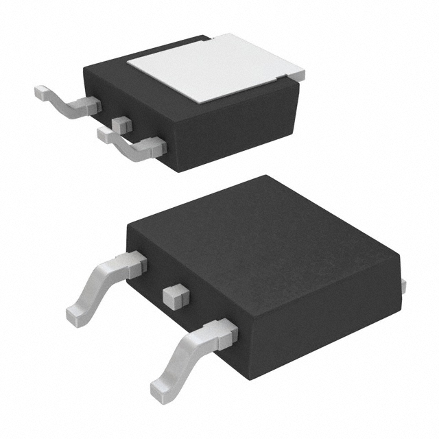
The SPD02N50C3 is an N-Channel MOSFET manufactured by Infineon Technologies, rated for 560V drain-to-source voltage with 1.8A continuous drain current. This device is part of the CoolMOS™ series and is packaged in TO-252-3 (DPAK) surface mount configuration with a maximum power dissipation of 25W.
The SPD02N50C3 is classified as Obsolete. Equivalent and substitute parts are necessary to maintain design continuity, ensure supply chain availability, and support ongoing production requirements for applications utilizing this component.
Substiute Parts
Key Parameters
| Parameter | Value | Unit |
|---|---|---|
| Drain-to-Source Voltage (Vdss) | 560 | V |
| Continuous Drain Current (Id) @ 25°C | 1.8 | A |
| On-State Resistance (Rds On) @ 1.1A, 10V | 3 | Ω |
| Gate Threshold Voltage (Vgs(th)) @ 80µA | 3.9 | V |
| Gate Charge (Qg) @ 10V | 9 | nC |
| Input Capacitance (Ciss) @ 25V | 190 | pF |
| Power Dissipation (Max) | 25 | W |
| Operating Temperature Range | -55 to 150 | °C |
| Package Type | TO-252-3 (DPAK) | — |
| Mounting Type | Surface Mount | — |
Substitute Part Grouping Explanation
Substitution of the SPD02N50C3 is determined by the following critical electrical and mechanical parameters:
Electrical Compatibility Criteria:
- Drain-to-Source Voltage (Vdss): Substitute parts must equal or exceed 500V minimum to maintain voltage margin
- Continuous Drain Current (Id): Substitute parts must equal or exceed 1.8A to support circuit current requirements
- On-State Resistance (Rds On): Substitute parts must not exceed 3.3Ω to maintain acceptable power dissipation and thermal performance
- Gate Threshold Voltage (Vgs(th)): Must be within ±1V of the original specification for gate drive compatibility
- Maximum Gate Voltage (Vgs): Substitute parts must support ±20V minimum gate drive voltage
- Operating Temperature Range: Must support -55°C to 150°C minimum
Mechanical Compatibility Criteria:
- Package Type: TO-252-3 (DPAK) surface mount configuration required
- Mounting Type: Surface mount only
- Moisture Sensitivity Level: MSL 1 (Unlimited) required
The three substitute parts listed (AOD3N50, STD3NK50ZT4, STD4N52K3) meet these criteria with the following considerations:
- AOD3N50: 500V Vdss, 2.8A Id, 3Ω Rds On, TO-252 package
- STD3NK50ZT4: 500V Vdss, 2.3A Id, 3.3Ω Rds On, DPAK package, Active product status
- STD4N52K3: 525V Vdss, 2.5A Id, 2.6Ω Rds On, DPAK package, Active product status
Parameter Comparison
| Parameter | SPD02N50C3 (Main) | AOD3N50 | STD3NK50ZT4 | STD4N52K3 |
|---|---|---|---|---|
| Manufacturer | Infineon Technologies | Alpha & Omega Semiconductor Inc. | STMicroelectronics | STMicroelectronics |
| Vdss (V) | 560 | 500 | 500 | 525 |
| Id @ 25°C (A) | 1.8 | 2.8 | 2.3 | 2.5 |
| Rds On @ 10V (Ω) | 3.0 | 3.0 | 3.3 | 2.6 |
| Vgs(th) (V) | 3.9 | 4.5 | 4.5 | 4.5 |
| Qg @ 10V (nC) | 9 | 8 | 15 | 2 |
| Ciss @ 25V (pF) | 190 | 331 | 280 | 334 |
| Power Dissipation (W) | 25 | 57 | 45 | 45 |
| Operating Temperature (°C) | -55 to 150 | -50 to 150 | -55 to 150 | -55 to 150 |
| Package | TO-252-3 (DPAK) | TO-252 (DPAK) | DPAK | DPAK |
| Product Status | Obsolete | Not For New Designs | Active | Active |
| RoHS Status | — | — | ROHS3 Compliant | ROHS3 Compliant |
Engineering Selection Recommendations
STD3NK50ZT4 and STD4N52K3 are the preferred substitutes for new designs and ongoing production:
- Both parts carry Active product status, ensuring long-term availability and supply chain stability
- Both parts are ROHS3 Compliant, meeting current environmental and regulatory requirements
- STD3NK50ZT4 maintains the closest electrical characteristics to the SPD02N50C3 with 500V Vdss and 2.3A Id
- STD4N52K3 offers superior on-state resistance (2.6Ω) and higher voltage rating (525V), providing enhanced performance margin
AOD3N50 is available as a secondary substitute option:
- Provides equivalent on-state resistance (3Ω) and higher current capability (2.8A)
- Classified as Not For New Designs; suitable for legacy system maintenance only
- Lower gate charge (8nC) compared to the main part
The SPD02N50C3 original part remains available in inventory (15,426 pcs) for immediate requirements. Transition planning should prioritize STD3NK50ZT4 or STD4N52K3 for long-term production continuity.
Frequently Asked Questions (FAQ)
Q: Can STD3NK50ZT4 directly replace SPD02N50C3 in existing designs?
A: STD3NK50ZT4 is electrically compatible within the specified parameter ranges. Both devices feature TO-252-3 (DPAK) surface mount packaging, identical pinout, and compatible gate drive voltage requirements (±30V vs. ±20V). The 500V Vdss rating of STD3NK50ZT4 is lower than the 560V rating of SPD02N50C3; circuit design must verify that the reduced voltage margin is acceptable for the application.
Q: What is the difference between AOD3N50 and STD3NK50ZT4?
A: AOD3N50 (Alpha & Omega Semiconductor) and STD3NK50ZT4 (STMicroelectronics) both feature 500V Vdss and TO-252 DPAK packaging. Key differences include: AOD3N50 has higher current capability (2.8A vs. 2.3A) and lower gate charge (8nC vs. 15nC), while STD3NK50ZT4 carries Active product status and ROHS3 compliance. AOD3N50 is classified as Not For New Designs.
Q: Why does STD4N52K3 have lower on-state resistance than the original SPD02N50C3?
A: STD4N52K3 features improved semiconductor technology (SuperMESH3™ series) that reduces on-state resistance to 2.6Ω while maintaining similar power dissipation ratings. This represents a performance enhancement in the substitute part. The higher voltage rating (525V) and lower gate charge (2nC) further indicate advanced device design.
Q: Are all substitute parts available in the same packaging?
A: All substitute parts use TO-252-3 (DPAK) surface mount packaging with identical pinout and footprint compatibility. Mechanical substitution is direct; no PCB layout modifications are required.
Q: What is the impact of higher input capacitance in substitute parts?
A: AOD3N50 and STD4N52K3 exhibit higher input capacitance (331pF and 334pF respectively) compared to SPD02N50C3 (190pF). This increases gate charge requirements and may affect switching speed in high-frequency applications. STD3NK50ZT4 (280pF) provides a middle ground. Circuit design must verify gate driver capability to support the increased capacitive load.
Q: Can I use these substitutes in new product designs?
A: STD3NK50ZT4 and STD4N52K3 are both classified as Active products and are suitable for new designs. AOD3N50 is classified as Not For New Designs and should be reserved for legacy system support only. For new product development, STD3NK50ZT4 or STD4N52K3 are the recommended selections.
Alternative Parts

SJ6012L2TP
Littelfuse Inc.
6 Alternative Parts

JMK107BBJ476MA-RE
Taiyo Yuden
10 Alternative Parts

GMK107BBJ475MA-T
Taiyo Yuden
5 Alternative Parts
SJ6020N2ARP
Littelfuse Inc.
3 Alternative Parts
SJ6025R2ATP
Littelfuse Inc.
4 Alternative Parts

2474-05L
API Delevan Inc.
1 Alternative Parts

4590R-684K
API Delevan Inc.
1 Alternative Parts

CM6560R-334
API Delevan Inc.
1 Alternative Parts

CM6460-104
API Delevan Inc.
1 Alternative Parts

5526-12
API Delevan Inc.
1 Alternative Parts