


Request Quote
(Ships tomorrow)
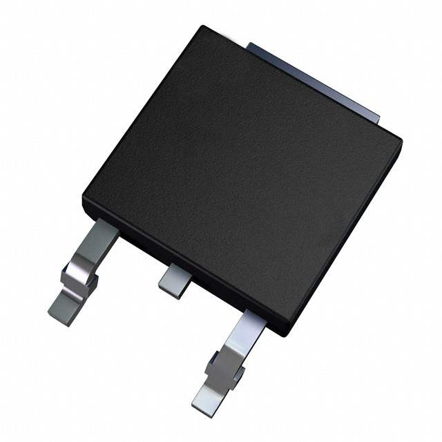
SFR9024TM P-Channel MOSFET Equivalent & Substitute Parts
Part Overview
The SFR9024TM is a P-Channel MOSFET manufactured by onsemi, rated for 60V drain-to-source voltage with 7.8A continuous drain current at 25°C. The device is housed in a TO-252AA (DPAK) surface mount package and is designed for general-purpose switching applications requiring moderate current handling and low on-resistance characteristics.
The SFR9024TM carries an Obsolete product status. Identifying equivalent and substitute parts is necessary to ensure design continuity, maintain supply chain reliability, and support ongoing production requirements for applications currently utilizing this component.
Substiute Parts
Key Parameters
| Parameter | Value | Unit |
|---|---|---|
| FET Type | P-Channel | — |
| Drain-to-Source Voltage (Vdss) | 60 | V |
| Continuous Drain Current (Id) @ 25°C | 7.8 | A (Tc) |
| On-Resistance (Rds On Max) @ Id, Vgs | 280 | mOhm @ 3.9A, 10V |
| Gate Threshold Voltage (Vgs(th) Max) @ Id | 4 | V @ 250µA |
| Gate Charge (Qg Max) @ Vgs | 19 | nC @ 10V |
| Maximum Gate Voltage (Vgs Max) | ±30 | V |
| Input Capacitance (Ciss Max) @ Vds | 600 | pF @ 25V |
| Power Dissipation (Max) | 2.5 (Ta), 32 (Tc) | W |
| Operating Temperature Range | -55 to 150 | °C (TJ) |
| Mounting Type | Surface Mount | — |
| Package | TO-252-3, DPAK (2 Leads + Tab), SC-63 | — |
| Moisture Sensitivity Level (MSL) | 1 (Unlimited) | — |
Substitute Part Grouping Explanation
Substitute parts for the SFR9024TM are selected based on strict electrical and mechanical compatibility criteria. The following parameters define acceptable substitution:
Primary Matching Criteria:
- FET Type: P-Channel (required)
- Drain-to-Source Voltage (Vdss): 60V (required)
- Package: TO-252-3, DPAK surface mount (required)
- Mounting Type: Surface Mount (required)
- Continuous Drain Current (Id): Equal to or greater than 7.8A (required)
Secondary Compatibility Parameters:
- Gate Threshold Voltage (Vgs(th)): Maximum 4V @ 250µA (required)
- Maximum Gate Voltage (Vgs Max): ±20V or greater (required)
- Operating Temperature Range: Minimum -55°C to 150°C (required)
- Moisture Sensitivity Level (MSL): 1 (Unlimited) (required)
All substitute parts listed meet these criteria and are electrically and mechanically compatible with the SFR9024TM in applications where the original component was specified.
Parameter Comparison
| Parameter | SFR9024TM (onsemi) | FQD11P06TM (onsemi) | SIHFR9024TR-GE3 (Vishay) | SPD08P06PGBTMA1 (Infineon) |
|---|---|---|---|---|
| Product Status | Obsolete | Active | Active | Active |
| FET Type | P-Channel | P-Channel | P-Channel | P-Channel |
| Vdss (V) | 60 | 60 | 60 | 60 |
| Id @ 25°C (A) | 7.8 (Tc) | 9.4 (Tc) | 8.8 (Tc) | 8.83 (Ta) |
| Rds On Max (mOhm) | 280 @ 3.9A, 10V | 185 @ 4.7A, 10V | 280 @ 5.3A, 10V | 300 @ 10A, 6.2V |
| Vgs(th) Max @ Id (V) | 4 @ 250µA | 4 @ 250µA | 4 @ 250µA | 4 @ 250µA |
| Gate Charge Qg Max (nC) | 19 @ 10V | 17 @ 10V | 19 @ 10V | 13 @ 10V |
| Vgs Max (V) | ±30 | ±30 | ±20 | ±20 |
| Ciss Max (pF) | 600 @ 25V | 550 @ 25V | 570 @ 25V | 420 @ 25V |
| Power Dissipation Max (W) | 2.5 (Ta), 32 (Tc) | 2.5 (Ta), 38 (Tc) | 2.5 (Ta), 42 (Tc) | 42 (Tc) |
| Operating Temperature (°C) | -55 to 150 | -55 to 150 | -55 to 150 | -55 to 175 |
| Package | TO-252-3, DPAK | TO-252-3, DPAK | TO-252-3, DPAK | TO-252-3, DPAK |
| RoHS Status | Not specified | ROHS3 Compliant | ROHS3 Compliant | ROHS3 Compliant |
| MSL | 1 (Unlimited) | 1 (Unlimited) | 1 (Unlimited) | 1 (Unlimited) |
| REACH Status | REACH Unaffected | Not specified | Not specified | REACH Unaffected |
Engineering Selection Recommendations
FQD11P06TM (onsemi QFET® Series)
The FQD11P06TM is an active product from onsemi with improved electrical performance relative to the SFR9024TM. It provides higher continuous drain current (9.4A versus 7.8A), lower on-resistance (185mOhm versus 280mOhm), and reduced gate charge (17nC versus 19nC). The device maintains identical gate threshold voltage, maximum gate voltage rating of ±30V, and operating temperature range. ROHS3 compliance and MSL 1 rating ensure regulatory and manufacturing compatibility. This substitute is suitable for direct replacement in applications where the enhanced current handling and reduced on-resistance provide design margin improvements.
SIHFR9024TR-GE3 (Vishay Siliconix)
The SIHFR9024TR-GE3 is an active product from Vishay Siliconix with electrical characteristics closely matched to the SFR9024TM. It provides 8.8A continuous drain current, identical on-resistance specification (280mOhm), and matching gate threshold voltage. The device features identical gate charge (19nC) and operating temperature range. The maximum gate voltage rating is ±20V, which is lower than the SFR9024TM (±30V) but remains within typical application requirements. ROHS3 compliance and MSL 1 rating confirm regulatory alignment. This substitute is suitable for applications requiring electrical equivalence with minimal performance variation.
SPD08P06PGBTMA1 (Infineon SIPMOS® Series)
The SPD08P06PGBTMA1 is an active product from Infineon Technologies with 8.83A continuous drain current and enhanced power dissipation capability (42W at Tc versus 32W). The device features lower gate charge (13nC versus 19nC) and reduced input capacitance (420pF versus 600pF), which may improve switching performance in high-frequency applications. The maximum gate voltage rating is ±20V. The operating temperature range extends to 175°C, providing additional thermal margin. ROHS3 compliance and REACH Unaffected status confirm regulatory compliance. This substitute is suitable for applications requiring enhanced thermal performance or reduced switching losses.
All three substitute parts are currently in active production status, ensuring long-term supply availability and design support compared to the obsolete SFR9024TM.
Frequently Asked Questions (FAQ)
Q: Can the FQD11P06TM directly replace the SFR9024TM in existing designs?
A: Yes. The FQD11P06TM is electrically and mechanically compatible with the SFR9024TM. Both devices share identical package geometry (TO-252-3, DPAK), gate threshold voltage (4V @ 250µA), and operating temperature range (-55°C to 150°C). The FQD11P06TM provides higher continuous drain current (9.4A versus 7.8A) and lower on-resistance (185mOhm versus 280mOhm), making it a performance-enhanced substitute suitable for direct replacement.
Q: What is the primary difference between the Vishay SIHFR9024TR-GE3 and the onsemi FQD11P06TM?
A: Both devices are electrically compatible with the SFR9024TM. The SIHFR9024TR-GE3 provides closer electrical equivalence to the original part, with matching on-resistance (280mOhm) and gate charge (19nC). The FQD11P06TM offers improved performance with lower on-resistance (185mOhm) and reduced gate charge (17nC). The SIHFR9024TR-GE3 has a maximum gate voltage rating of ±20V, while the FQD11P06TM maintains ±30V. Selection depends on whether design requirements prioritize electrical equivalence or performance enhancement.
Q: Is the Infineon SPD08P06PGBTMA1 suitable for high-temperature applications?
A: Yes. The SPD08P06PGBTMA1 supports an operating temperature range of -55°C to 175°C, extending 25°C beyond the SFR9024TM specification (-55°C to 150°C). This additional thermal margin makes it suitable for applications requiring higher junction temperature operation. The device also provides enhanced power dissipation capability (42W at Tc) compared to the SFR9024TM (32W at Tc).
Q: Are all substitute parts RoHS compliant?
A: Yes. The FQD11P06TM, SIHFR9024TR-GE3, and SPD08P06PGBTMA1 are all ROHS3 compliant. The SFR9024TM does not specify RoHS status. All substitute parts carry MSL 1 (Unlimited) moisture sensitivity rating, ensuring compatibility with standard manufacturing and storage practices.
Q: What is the impact of lower gate charge on circuit performance?
A: Lower gate charge reduces the energy required to switch the MOSFET on and off, which decreases switching losses and allows for faster switching transitions. The SPD08P06PGBTMA1 features the lowest gate charge (13nC) among the substitute options, followed by the FQD11P06TM (17nC). This characteristic is beneficial in high-frequency switching applications or designs where power efficiency is critical. The SFR9024TM and SIHFR9024TR-GE3 both specify 19nC gate charge.
Q: Can the maximum gate voltage difference (±30V versus ±20V) affect circuit design?
A: The maximum gate voltage rating defines the safe operating limit for gate-source voltage. The SFR9024TM and FQD11P06TM support ±30V, while the SIHFR9024TR-GE3 and SPD08P06PGBTMA1 support ±20V. In typical applications using standard gate drive circuits (±10V to ±15V), this difference has no practical impact. Applications requiring gate voltages exceeding ±20V must use the FQD11P06TM or SFR9024TM. Standard switching applications operate well within the ±20V limit of all substitute parts.
Q: What packaging considerations apply to these substitute parts?
A: All substitute parts use the TO-252-3 DPAK surface mount package with identical pin configuration and thermal characteristics. PCB layout, solder reflow profiles, and thermal management approaches remain unchanged. No design modifications are required for package compatibility. All devices carry MSL 1 (Unlimited) rating, indicating no moisture sensitivity restrictions during storage or handling.
Q: Which substitute part offers the best overall performance improvement?
A: The FQD11P06TM provides the most significant performance enhancement, combining higher continuous drain current (9.4A), lower on-resistance (185mOhm), and reduced gate charge (17nC). The SPD08P06PGBTMA1 offers the lowest gate charge (13nC) and highest operating temperature range (175°C), making it optimal for high-frequency or high-temperature applications. Selection depends on specific application requirements: general-purpose replacement favors the FQD11P06TM, while thermally demanding or high-frequency designs benefit from the SPD08P06PGBTMA1.
Alternative Parts

SJ6012L2TP
Littelfuse Inc.
6 Alternative Parts

JMK107BBJ476MA-RE
Taiyo Yuden
10 Alternative Parts

GMK107BBJ475MA-T
Taiyo Yuden
5 Alternative Parts
SJ6020N2ARP
Littelfuse Inc.
3 Alternative Parts
SJ6025R2ATP
Littelfuse Inc.
4 Alternative Parts

2474-05L
API Delevan Inc.
1 Alternative Parts

4590R-684K
API Delevan Inc.
1 Alternative Parts

CM6560R-334
API Delevan Inc.
1 Alternative Parts

CM6460-104
API Delevan Inc.
1 Alternative Parts

5526-12
API Delevan Inc.
1 Alternative Parts