


Request Quote
(Ships tomorrow)
SA5532P Equivalent & Substitute Parts
Part Overview
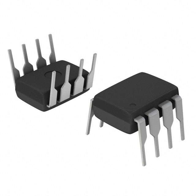
The SA5532P is a general-purpose operational amplifier manufactured by Texas Instruments, housed in an 8-DIP package for through-hole mounting. This dual-circuit linear amplifier is designed for applications requiring moderate bandwidth and low noise characteristics. The device is currently in active production status with 2351 units available in stock.
Substitute parts become necessary when the primary component experiences supply constraints, extended lead times, or when design requirements permit operation within broader electrical parameter ranges. The SA5532P has two manufacturer-recommended equivalents that maintain functional compatibility while offering alternative supply sources and performance characteristics.
Substiute Parts
Key Parameters
| Parameter | Value | Unit |
|---|---|---|
| Amplifier Type | General Purpose | — |
| Number of Circuits | 2 | — |
| Slew Rate | 9 | V/µs |
| Gain Bandwidth Product | 10 | MHz |
| Current - Input Bias | 200 | nA |
| Voltage - Input Offset | 500 | µV |
| Current - Supply (x2 Channels) | 8 | mA |
| Current - Output / Channel | 38 | mA |
| Voltage - Supply Span (Min) | 10 | V |
| Voltage - Supply Span (Max) | 30 | V |
| Operating Temperature | -40 to 85 | °C |
| Package / Case | 8-DIP (0.300", 7.62mm) | — |
| Mounting Type | Through Hole | — |
| RoHS Status | ROHS3 Compliant | — |
Substitute Part Grouping Explanation
Substitution compatibility for the SA5532P is determined by the following critical parameters:
Package and Pinout Compatibility: All substitute parts must use the 8-DIP (0.300", 7.62mm) through-hole package to ensure direct board-level replacement without layout modifications.
Dual-Circuit Configuration: The SA5532P contains two independent operational amplifier circuits. Substitute parts must maintain this dual-circuit architecture to preserve functional equivalence.
Supply Voltage Range: The SA5532P operates across a 10V to 30V supply span. Substitute parts with broader supply ranges (such as 3V to 36V) remain compatible within the original operating envelope.
Output Current Capability: The SA5532P delivers 38mA per channel. Substitute parts with equal or greater output current capacity (40mA or higher) satisfy this requirement.
Thermal Operating Range: All substitute parts must support the -40°C to 85°C operating temperature range.
Regulatory Compliance: All parts must maintain ROHS3 compliance and REACH unaffected status to meet procurement and environmental standards.
The two manufacturer-recommended substitutes—AS358AP-E1 and NJM4580D—satisfy these core compatibility criteria while offering distinct performance trade-offs in slew rate, input bias current, and supply current consumption.
Parameter Comparison
| Parameter | SA5532P (Main) | AS358AP-E1 | NJM4580D | Unit |
|---|---|---|---|---|
| Manufacturer | Texas Instruments | Diodes Incorporated | Nisshinbo Micro Devices Inc. | — |
| Amplifier Type | General Purpose | General Purpose | Audio | — |
| Number of Circuits | 2 | 2 | 2 | — |
| Slew Rate | 9 | Not Specified | 5 | V/µs |
| Gain Bandwidth Product | 10 | Not Specified | 15 | MHz |
| Current - Input Bias | 200 | 20 | 100 | nA |
| Voltage - Input Offset | 500 | 2000 | 500 | µV |
| Current - Supply (x2 Channels) | 8 | 0.7 | 6 | mA |
| Current - Output / Channel | 38 | 40 | 50 | mA |
| Voltage - Supply Span (Min) | 10 | 3 | 4 | V |
| Voltage - Supply Span (Max) | 30 | 36 | 36 | V |
| Operating Temperature | -40 to 85 | -40 to 85 | -40 to 85 | °C |
| Package / Case | 8-DIP (0.300", 7.62mm) | 8-DIP (0.300", 7.62mm) | 8-DIP (0.300", 7.62mm) | — |
| Mounting Type | Through Hole | Through Hole | Through Hole | — |
| Product Status | Active | Active | Not For New Designs | — |
| RoHS Status | ROHS3 Compliant | ROHS3 Compliant | RoHS Compliant | — |
Engineering Selection Recommendations
AS358AP-E1 (Diodes Incorporated): This substitute offers the lowest input bias current (20nA) and the lowest supply current consumption (0.7mA across both channels), making it suitable for battery-powered or low-power applications. The AS358AP-E1 maintains active product status and ROHS3 compliance. The broader minimum supply voltage (3V) permits operation in lower-voltage systems while remaining compatible within the SA5532P's 10V to 30V envelope. The higher input offset voltage (2mV versus 500µV) represents a trade-off in precision but remains acceptable for general-purpose amplification. Output current capability (40mA) exceeds the SA5532P requirement.
NJM4580D (Nisshinbo Micro Devices Inc.): This substitute is classified as "Not For New Designs," indicating that Nisshinbo has discontinued active development for this component. While the NJM4580D remains in stock (45300 units), its use is restricted to legacy system maintenance and repair applications. The device offers higher gain bandwidth product (15MHz versus 10MHz) and greater output current per channel (50mA). Supply current consumption (6mA) falls between the SA5532P and AS358AP-E1. The lower slew rate (5V/µs versus 9V/µs) may limit performance in high-speed signal conditioning applications.
Recommendation for New Designs: The AS358AP-E1 is the preferred substitute for new product development due to its active status, superior power efficiency, and ROHS3 compliance. The NJM4580D is suitable only for sustaining existing systems where component replacement is necessary.
Frequently Asked Questions (FAQ)
Q: Can the AS358AP-E1 directly replace the SA5532P on existing PCBs?
A: Yes. Both devices use identical 8-DIP (0.300", 7.62mm) through-hole packaging with the same pinout configuration. No PCB layout modifications are required for direct substitution.
Q: What is the significance of the AS358AP-E1's lower input bias current?
A: The AS358AP-E1 draws only 20nA of input bias current compared to the SA5532P's 200nA. This characteristic reduces loading on high-impedance signal sources and decreases power consumption in battery-powered applications. For standard general-purpose amplification, this difference has minimal impact on circuit performance.
Q: Why is the NJM4580D marked "Not For New Designs"?
A: This designation indicates that Nisshinbo Micro Devices has ceased active development and qualification of this component. While existing inventory remains available for legacy system support, the manufacturer does not recommend its use in new product development. Future availability cannot be guaranteed.
Q: How does the AS358AP-E1's higher input offset voltage affect circuit performance?
A: The AS358AP-E1 exhibits 2mV input offset voltage compared to the SA5532P's 500µV. In general-purpose amplification circuits, this difference is typically compensated through standard offset nulling techniques or is negligible relative to signal levels. In precision instrumentation requiring sub-millivolt accuracy, the SA5532P remains the preferred choice.
Q: Are all three parts RoHS compliant?
A: The SA5532P and AS358AP-E1 are ROHS3 compliant. The NJM4580D is RoHS compliant but does not carry the ROHS3 designation. Both compliance levels satisfy current environmental regulations; ROHS3 represents the most recent standard revision.
Q: What supply voltage range should be used for substitution?
A: All three parts operate safely within the SA5532P's original 10V to 30V supply range. The AS358AP-E1 and NJM4580D support broader ranges (3V to 36V and 4V to 36V respectively), but operation outside the original 10V to 30V envelope requires circuit re-evaluation and is not necessary for direct substitution.
Q: Can the NJM4580D be used in new designs if inventory is available?
A: No. The "Not For New Designs" status is a manufacturer directive that supersedes inventory availability. This classification reflects the manufacturer's decision to discontinue support and qualification for new applications. Use of this component in new designs creates long-term supply and support risks.
Alternative Parts

SJ6012L2TP
Littelfuse Inc.
6 Alternative Parts

JMK107BBJ476MA-RE
Taiyo Yuden
10 Alternative Parts

GMK107BBJ475MA-T
Taiyo Yuden
5 Alternative Parts
SJ6020N2ARP
Littelfuse Inc.
3 Alternative Parts
SJ6025R2ATP
Littelfuse Inc.
4 Alternative Parts

2474-05L
API Delevan Inc.
1 Alternative Parts

4590R-684K
API Delevan Inc.
1 Alternative Parts

CM6560R-334
API Delevan Inc.
1 Alternative Parts

CM6460-104
API Delevan Inc.
1 Alternative Parts

5526-12
API Delevan Inc.
1 Alternative Parts