


Request Quote
(Ships tomorrow)
SA5230DR2G Equivalent & Substitute Parts
Part Overview
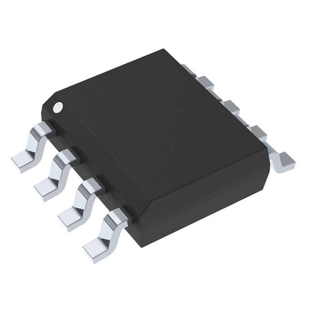
The SA5230DR2G is a general-purpose operational amplifier manufactured by onsemi, housed in an 8-SOIC surface mount package. This device features rail-to-rail output capability and is designed for linear amplification applications requiring low-power operation across a wide supply voltage range. The SA5230DR2G is classified as obsolete, making identification of functionally equivalent alternatives necessary for ongoing design support and procurement continuity.
Substiute Parts
Key Parameters
| Parameter | Value | Unit |
|---|---|---|
| Amplifier Type | General Purpose | — |
| Number of Circuits | 1 | — |
| Output Type | Rail-to-Rail | — |
| Slew Rate | 0.25 | V/µs |
| Gain Bandwidth Product | 600 | kHz |
| Current - Input Bias | 40 | nA |
| Voltage - Input Offset | 400 | µV |
| Current - Supply | 1.1 | mA |
| Current - Output / Channel | 32 | mA |
| Voltage - Supply Span (Min) | 1.8 | V |
| Voltage - Supply Span (Max) | 15 | V |
| Operating Temperature Range | -40 to 85 | °C |
| Package / Case | 8-SOIC (0.154", 3.90mm Width) | — |
| Mounting Type | Surface Mount | — |
| Moisture Sensitivity Level | 1 (Unlimited) | — |
Substitute Part Grouping Explanation
Substitution of the SA5230DR2G is determined by equivalence across the following critical parameters:
Functional Equivalence Criteria:
- Amplifier type classification (General Purpose)
- Number of circuits (single-channel configuration)
- Output architecture (Rail-to-Rail capability)
- Package form factor (8-SOIC surface mount)
- Moisture sensitivity level (MSL 1)
Electrical Compatibility Criteria:
- Slew rate performance (0.25 V/µs minimum)
- Gain bandwidth product (600 kHz minimum)
- Input bias current specification
- Input offset voltage specification
- Output current capability per channel
- Supply voltage operating range overlap
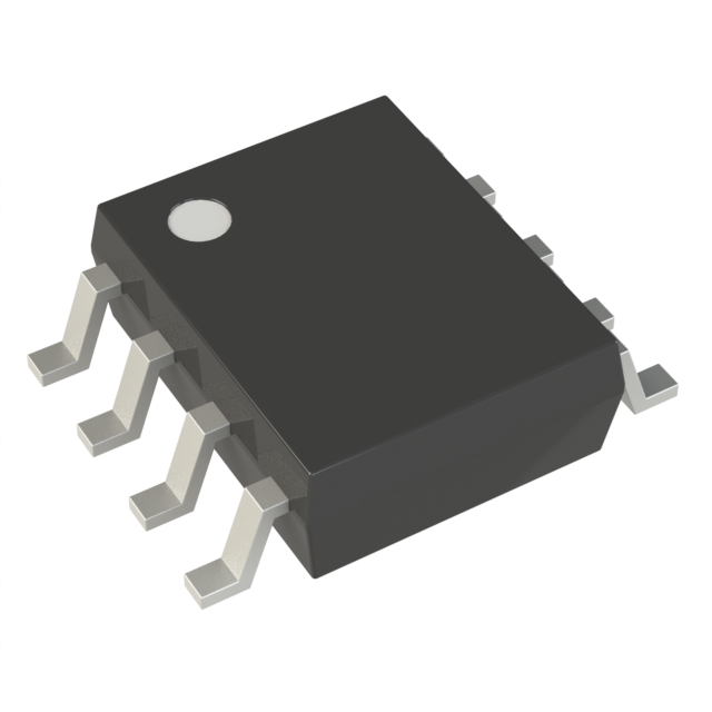
The TS1851IDT from STMicroelectronics meets all functional equivalence criteria and demonstrates electrical compatibility within the specified parameter ranges.
Parameter Comparison
| Parameter | SA5230DR2G (onsemi) | TS1851IDT (STMicroelectronics) | Unit |
|---|---|---|---|
| Amplifier Type | General Purpose | General Purpose | — |
| Number of Circuits | 1 | 1 | — |
| Output Type | Rail-to-Rail | Rail-to-Rail | — |
| Slew Rate | 0.25 | 0.25 | V/µs |
| Gain Bandwidth Product | 600 | 630 | kHz |
| Current - Input Bias | 40 | 16 | nA |
| Voltage - Input Offset | 400 | 1000 | µV |
| Current - Supply | 1.1 | 0.162 | mA |
| Current - Output / Channel | 32 | 48 | mA |
| Voltage - Supply Span (Min) | 1.8 | 1.8 | V |
| Voltage - Supply Span (Max) | 15 | 6 | V |
| Operating Temperature Range | -40 to 85 | -40 to 125 | °C |
| Package / Case | 8-SOIC (0.154", 3.90mm Width) | 8-SOIC (0.154", 3.90mm Width) | — |
| Mounting Type | Surface Mount | Surface Mount | — |
| Moisture Sensitivity Level | 1 (Unlimited) | 1 (Unlimited) | — |
Engineering Selection Recommendations
Product Status Consideration: The SA5230DR2G is classified as obsolete, whereas the TS1851IDT is active in production. For new designs and ongoing procurement, the TS1851IDT provides continuity of supply and manufacturer support.
Compliance and Certification: The TS1851IDT holds RoHS3 compliance certification, whereas the SA5230DR2G does not specify RoHS status. Both devices are REACH Unaffected and carry EAR99 ECCN classification. Both are classified under HTSUS code 8542.33.0001.
Electrical Performance: The TS1851IDT demonstrates superior performance in several parameters: lower input bias current (16 nA versus 40 nA), higher output current capability (48 mA versus 32 mA), and lower quiescent supply current (162 µA versus 1.1 mA). The TS1851IDT operates across a narrower maximum supply voltage range (6 V maximum versus 15 V maximum for the SA5230DR2G). Applications requiring supply voltages exceeding 6 V require design modification or alternative selection.
Temperature Range: The TS1851IDT supports an extended operating temperature range (-40°C to 125°C) compared to the SA5230DR2G (-40°C to 85°C), providing broader environmental applicability.
Package Compatibility: Both devices utilize identical 8-SOIC surface mount packaging with 0.154" (3.90 mm) width, enabling direct footprint compatibility on printed circuit boards.
Frequently Asked Questions (FAQ)
Q: Can the TS1851IDT directly replace the SA5230DR2G in existing designs?
A: Direct replacement is possible for applications operating at supply voltages of 6 V or lower. The TS1851IDT maximum supply voltage is 6 V, whereas the SA5230DR2G supports up to 15 V. Designs utilizing supply voltages exceeding 6 V require alternative component selection or circuit redesign.
Q: What are the key electrical differences between these devices?
A: The TS1851IDT exhibits lower input bias current (16 nA versus 40 nA), higher output current capability (48 mA versus 32 mA), and significantly lower quiescent supply current (162 µA versus 1.1 mA). The TS1851IDT has a slightly higher gain bandwidth product (630 kHz versus 600 kHz). Input offset voltage is higher in the TS1851IDT (1 mV versus 400 µV).
Q: Are the packages identical?
A: Yes. Both the SA5230DR2G and TS1851IDT are housed in 8-SOIC surface mount packages with identical dimensions (0.154" or 3.90 mm width). PCB footprints are directly compatible.
Q: What is the moisture sensitivity level for both devices?
A: Both devices are classified as MSL 1 (Unlimited), indicating no moisture sensitivity restrictions during storage or handling.
Q: Does the TS1851IDT meet regulatory compliance requirements?
A: The TS1851IDT is RoHS3 compliant and REACH Unaffected. Both devices carry EAR99 ECCN classification and are categorized under HTSUS code 8542.33.0001.
Q: What is the operating temperature range difference?
A: The SA5230DR2G operates from -40°C to 85°C. The TS1851IDT operates from -40°C to 125°C, providing a 40°C extended upper temperature limit.
Q: Is the TS1851IDT suitable for low-power applications?
A: Yes. The TS1851IDT demonstrates significantly lower quiescent supply current (162 µA) compared to the SA5230DR2G (1.1 mA), making it more suitable for battery-powered and low-power applications.
Alternative Parts

SJ6012L2TP
Littelfuse Inc.
6 Alternative Parts

JMK107BBJ476MA-RE
Taiyo Yuden
10 Alternative Parts

GMK107BBJ475MA-T
Taiyo Yuden
5 Alternative Parts
SJ6020N2ARP
Littelfuse Inc.
3 Alternative Parts
SJ6025R2ATP
Littelfuse Inc.
4 Alternative Parts

2474-05L
API Delevan Inc.
1 Alternative Parts

4590R-684K
API Delevan Inc.
1 Alternative Parts

CM6560R-334
API Delevan Inc.
1 Alternative Parts

CM6460-104
API Delevan Inc.
1 Alternative Parts

5526-12
API Delevan Inc.
1 Alternative Parts