


Request Quote
(Ships tomorrow)
PMGD280UN,115 Equivalent & Substitute Parts
Part Overview
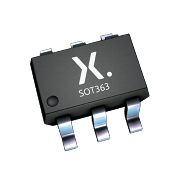
The PMGD280UN,115 is a dual N-channel MOSFET array manufactured by Nexperia USA Inc., designed for surface mount applications in the 6-TSSOP package. This device features a 20V drain-to-source voltage rating, 870mA continuous drain current, and 400mW maximum power dissipation. The part operates across an industrial temperature range of -55°C to 150°C and incorporates logic level gate drive capability.
The PMGD280UN,115 carries a product status of "Not For New Designs," indicating that Nexperia has discontinued active development for this component. This status necessitates identification of functionally equivalent alternatives that maintain electrical and mechanical compatibility for existing applications or new designs requiring similar performance characteristics.
Substiute Parts
Key Parameters
| Parameter | Value | Unit |
|---|---|---|
| Drain to Source Voltage (Vdss) | 20 | V |
| Continuous Drain Current (Id) @ 25°C | 870 | mA |
| On-State Resistance (Rds On) @ 200mA, 4.5V | 340 | mOhm |
| Gate Threshold Voltage (Vgs(th)) @ 250µA | 1 | V |
| Gate Charge (Qg) @ 4.5V | 0.89 | nC |
| Input Capacitance (Ciss) @ 20V | 45 | pF |
| Maximum Power Dissipation | 400 | mW |
| Operating Temperature Range | -55 to 150 | °C |
| Configuration | 2 N-Channel (Dual) | — |
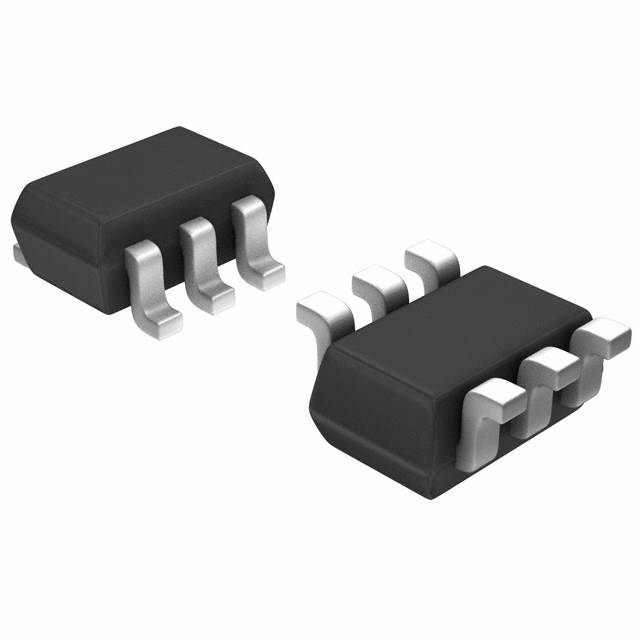
| Package Type | 6-TSSOP / SC-88 / SOT-363 | — |
| Mounting Type | Surface Mount | — |
Substitute Part Grouping Explanation
Substitution of the PMGD280UN,115 is determined by strict adherence to the following electrical and mechanical parameters:
Primary Substitution Criteria:
- Drain-to-source voltage (Vdss) must equal or exceed 20V
- Configuration must be dual N-channel (2 N-Channel)
- Package must be compatible with 6-TSSOP, SC-88, or SOT-363 footprints
- Operating temperature range must span -55°C to 150°C
- Logic level gate drive capability must be present
- Surface mount mounting type required
Secondary Compatibility Factors:
- Continuous drain current (Id) should meet or exceed application requirements
- On-state resistance (Rds On) affects thermal performance and power dissipation
- Gate charge (Qg) and input capacitance (Ciss) influence switching speed and gate drive requirements
- Maximum power dissipation rating must support the thermal environment
The substitute parts listed below satisfy all primary criteria and maintain electrical compatibility within the specified parameter ranges. Variations in secondary parameters reflect different manufacturing technologies and design approaches across manufacturers while preserving functional equivalence.
Parameter Comparison
| Parameter | PMGD280UN,115 (Nexperia) | BSD235NH6327XTSA1 (Infineon) | BSD840NH6327XTSA1 (Infineon) | FDG6317NZ (onsemi) | NTJD4401NT1G (onsemi) | NVJD4401NT1G (onsemi) | PJT7800_R1_00001 (Panjit) |
|---|---|---|---|---|---|---|---|
| Vdss (V) | 20 | 20 | 20 | 20 | 20 | 20 | 20 |
| Id @ 25°C (mA) | 870 | 950 | 880 | 700 | 630 | 630 | 1000 |
| Rds On (mOhm) | 340 @ 200mA, 4.5V | 350 @ 950mA, 4.5V | 400 @ 880mA, 2.5V | 400 @ 700mA, 4.5V | 375 @ 630mA, 4.5V | 375 @ 630mA, 4.5V | 150 @ 1A, 4.5V |
| Vgs(th) (V) | 1 @ 250µA | 1.2 @ 1.6µA | 0.75 @ 1.6µA | 1.5 @ 250µA | 1.5 @ 250µA | 1.5 @ 250µA | 1 @ 250µA |
| Qg (nC) | 0.89 @ 4.5V | 0.32 @ 4.5V | 0.26 @ 2.5V | 1.1 @ 4.5V | 3 @ 4.5V | 3 @ 4.5V | 1.6 @ 4.5V |
| Ciss (pF) | 45 @ 20V | 63 @ 10V | 78 @ 10V | 66.5 @ 10V | 46 @ 20V | 46 @ 20V | 92 @ 10V |
| Power Max (mW) | 400 | 500 | 500 | 300 | 270 | 270 | 350 |
| Operating Temp (°C) | -55 to 150 | -55 to 150 | -55 to 150 | -55 to 150 | -55 to 150 | -55 to 150 | -55 to 150 |
| Configuration | 2 N-Channel | 2 N-Channel | 2 N-Channel | 2 N-Channel | 2 N-Channel | 2 N-Channel | 2 N-Channel |
| Package | 6-TSSOP / SC-88 / SOT-363 | 6-VSSOP / SC-88 / SOT-363 | 6-VSSOP / SC-88 / SOT-363 | 6-TSSOP / SC-88 / SOT-363 | 6-TSSOP / SC-88 / SOT-363 | 6-TSSOP / SC-88 / SOT-363 | 6-TSSOP / SC-88 / SOT-363 |
| Product Status | Not For New Designs | Active | Active | Last Time Buy | Active | Active | Active |
| RoHS Compliance | ROHS3 | ROHS3 | ROHS3 | ROHS3 | ROHS3 | ROHS3 | ROHS3 |
| AEC-Q101 Qualified | No | Yes | No | No | No | Yes | No |
Engineering Selection Recommendations
Primary Substitutes (Active Product Status):
The BSD235NH6327XTSA1 (Infineon OptiMOS™ 2) and NTJD4401NT1G / NVJD4401NT1G (onsemi) represent the most suitable alternatives for new designs. These parts maintain active product status with full manufacturer support and availability. The BSD235NH6327XTSA1 offers superior performance with 950mA continuous drain current and reduced gate charge (0.32nC), making it ideal for applications requiring higher current capacity or faster switching. The NVJD4401NT1G provides AEC-Q101 automotive qualification, suitable for automotive and harsh environment applications.
Secondary Substitutes (Limited Availability):
The PJT7800_R1_00001 (Panjit) delivers the highest continuous drain current (1A) and lowest on-state resistance (150mOhm), providing enhanced performance for power-sensitive applications. However, this part carries active status with standard commercial availability.
The FDG6317NZ (onsemi PowerTrench®) maintains compatibility but carries "Last Time Buy" status, indicating limited future availability. This part is suitable only for applications where existing inventory can be secured or where near-term production completion is planned.
Compliance Considerations:
All substitute parts maintain ROHS3 compliance and REACH unaffected status, matching the environmental regulatory profile of the original PMGD280UN,115. The BSD235NH6327XTSA1 and NVJD4401NT1G include AEC-Q101 automotive qualification, providing additional assurance for mission-critical applications.
Frequently Asked Questions (FAQ)
Q: Can the PMGD280UN,115 be directly replaced with any of these substitutes without PCB modification?
A: Yes, all listed substitutes are compatible with the same 6-TSSOP / SC-88 / SOT-363 footprint. Direct PCB replacement is possible without layout changes. However, verify that the specific package variant (6-TSSOP, 6-VSSOP, or SOT-363) matches your PCB design, as some manufacturers offer multiple package options.
Q: What is the difference between the NTJD4401NT1G and NVJD4401NT1G?
A: Both parts are electrically identical with matching electrical specifications. The NVJD4401NT1G includes AEC-Q101 automotive qualification, making it suitable for automotive applications. The NTJD4401NT1G is the commercial-grade equivalent. Select based on application requirements.
Q: Why does the PJT7800_R1_00001 have significantly lower on-state resistance?
A: The PJT7800_R1_00001 employs a different die design and manufacturing process that achieves lower on-state resistance (150mOhm versus 340-400mOhm in other parts). This results in reduced power dissipation and heat generation, beneficial for high-current applications. The trade-off is higher input capacitance (92pF), which may require stronger gate drive capability.
Q: Is the PMGD280UN,115 still available for purchase?
A: The PMGD280UN,115 carries "Not For New Designs" status from Nexperia, indicating discontinued active development. Existing inventory may be available through authorized distributors, but long-term availability is not guaranteed. New designs should transition to active alternatives such as the BSD235NH6327XTSA1 or NTJD4401NT1G.
Q: What does "Last Time Buy" status mean for the FDG6317NZ?
A: "Last Time Buy" indicates that onsemi has announced end-of-life for this product. Customers have a final opportunity to purchase remaining inventory before production ceases. This part should not be selected for new designs unless existing stock can be secured for the entire production run.
Q: Are there thermal performance differences between these substitutes?
A: Yes. The PJT7800_R1_00001 exhibits the lowest thermal resistance due to its 150mOhm on-state resistance, generating less heat at equivalent current levels. The NTJD4401NT1G and NVJD4401NT1G generate more heat (375mOhm resistance) but are suitable for lower-current applications. Thermal design must account for the specific part selected and the application's current profile.
Q: Can I use the BSD840NH6327XTSA1 as a substitute?
A: The BSD840NH6327XTSA1 meets all electrical and mechanical compatibility criteria and is functionally equivalent. However, it carries active product status without AEC-Q101 qualification. It is suitable for commercial applications but not recommended for automotive or mission-critical environments requiring automotive-grade components.
Q: What is the significance of gate charge (Qg) differences?
A: Gate charge determines the energy required to switch the MOSFET on and off. Lower gate charge (BSD840NH6327XTSA1 at 0.26nC) requires less gate drive power and enables faster switching. Higher gate charge (NTJD4401NT1G at 3nC) requires stronger gate drive capability but may be acceptable in applications with adequate drive circuitry. Select based on gate driver specifications and switching frequency requirements.
Q: Are all substitutes RoHS3 compliant?
A: Yes, all listed substitute parts maintain ROHS3 compliance, matching the environmental regulatory status of the PMGD280UN,115. All parts are also REACH unaffected, ensuring compliance with European chemical regulations.
Alternative Parts

SJ6012L2TP
Littelfuse Inc.
6 Alternative Parts

JMK107BBJ476MA-RE
Taiyo Yuden
10 Alternative Parts

GMK107BBJ475MA-T
Taiyo Yuden
5 Alternative Parts
SJ6020N2ARP
Littelfuse Inc.
3 Alternative Parts
SJ6025R2ATP
Littelfuse Inc.
4 Alternative Parts

2474-05L
API Delevan Inc.
1 Alternative Parts

4590R-684K
API Delevan Inc.
1 Alternative Parts

CM6560R-334
API Delevan Inc.
1 Alternative Parts

CM6460-104
API Delevan Inc.
1 Alternative Parts

5526-12
API Delevan Inc.
1 Alternative Parts