


Request Quote
(Ships tomorrow)
PMDPB70EN,115 Equivalent & Substitute Parts
Part Overview
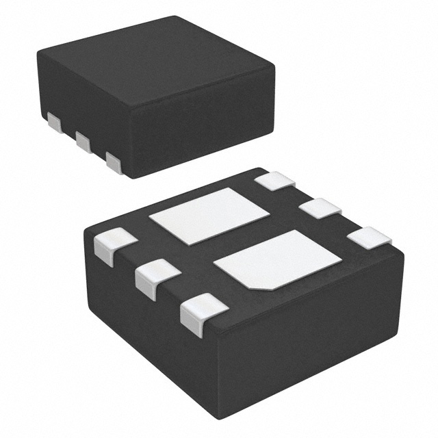
The PMDPB70EN,115 is a dual N-channel MOSFET array manufactured by Nexperia USA Inc., rated for 30V drain-to-source voltage and 3.5A continuous drain current. This surface mount component features logic level gate operation and is housed in a 6-HUSON (2x2) package. The part is classified as obsolete, necessitating identification of active equivalent alternatives that maintain electrical and mechanical compatibility for ongoing production and repair applications.
Substiute Parts
Key Parameters
| Parameter | Value | Unit |
|---|---|---|
| Drain to Source Voltage (Vdss) | 30 | V |
| Continuous Drain Current (Id) @ 25°C | 3.5 | A |
| Rds On (Max) @ Id, Vgs | 57 @ 3.5A, 10V | mOhm |
| Vgs(th) (Max) @ Id | 2.5 @ 250µA | V |
| Gate Charge (Qg) (Max) @ Vgs | 4.5 @ 10V | nC |
| Input Capacitance (Ciss) (Max) @ Vds | 130 @ 15V | pF |
| Power Dissipation (Max) | 510 | mW |
| Operating Temperature Range | -55 to 150 | °C (TJ) |
| Configuration | 2 N-Channel (Dual) | — |
| FET Feature | Logic Level Gate | — |
| Mounting Type | Surface Mount | — |
| Package / Case | 6-UFDFN Exposed Pad | — |
| RoHS Status | ROHS3 Compliant | — |
| Moisture Sensitivity Level (MSL) | 1 (Unlimited) | — |
Substitute Part Grouping Explanation
Substitution of the PMDPB70EN,115 is determined by strict alignment of the following electrical and mechanical parameters:
Critical Matching Parameters:
- Drain-to-source voltage rating (Vdss): 30V minimum
- Continuous drain current (Id): 3.5A or greater at 25°C
- Configuration: Dual N-channel (2 N-CH)
- Gate feature: Logic level operation
- Mounting: Surface mount technology
- Package type: 6-pin dual (2x2) footprint variants
- Compliance: ROHS3 and MSL Level 1
Acceptable Variation Ranges:
- Rds On: Substitute values must not exceed the maximum specified for the application circuit
- Gate charge and input capacitance: Variations acceptable within circuit switching requirements
- Power dissipation: Substitute ratings of 510mW or higher are acceptable
- Operating temperature: -55°C to 150°C minimum range required
The identified substitute parts meet these criteria while offering active product status and improved or equivalent electrical performance.
Parameter Comparison
| Parameter | PMDPB70EN,115 (Nexperia) | IRLHS6376TRPBF (Infineon) | SSM6N55NU,LF (Toshiba) |
|---|---|---|---|
| Manufacturer | Nexperia USA Inc. | Infineon Technologies | Toshiba Semiconductor and Storage |
| Product Status | Obsolete | Active | Active |
| Vdss (V) | 30 | 30 | 30 |
| Id @ 25°C (A) | 3.5 | 3.6 | 4.0 |
| Rds On (Max) (mOhm) | 57 @ 3.5A, 10V | 63 @ 3.4A, 4.5V | 46 @ 4A, 10V |
| Vgs(th) (Max) (V) | 2.5 @ 250µA | 1.1 @ 10µA | 2.5 @ 100µA |
| Gate Charge (Qg) (Max) (nC) | 4.5 @ 10V | 2.8 @ 4.5V | 2.5 @ 4.5V |
| Input Capacitance (Ciss) (Max) (pF) | 130 @ 15V | 270 @ 25V | 280 @ 15V |
| Power Dissipation (Max) (mW) | 510 | 1500 | 1000 |
| Configuration | 2 N-Channel (Dual) | 2 N-Channel (Dual) | 2 N-Channel (Dual) |
| FET Feature | Logic Level Gate | Logic Level Gate | Logic Level Gate |
| Operating Temperature (°C) | -55 to 150 | -55 to 150 | -55 to 150 |
| Mounting Type | Surface Mount | Surface Mount | Surface Mount |
| Package / Case | 6-UFDFN Exposed Pad | 6-PowerVDFN | 6-WDFN Exposed Pad |
| RoHS Status | ROHS3 Compliant | ROHS3 Compliant | ROHS3 Compliant |
| MSL | 1 (Unlimited) | 1 (Unlimited) | 1 (Unlimited) |
Engineering Selection Recommendations
IRLHS6376TRPBF (Infineon Technologies)
The IRLHS6376TRPBF qualifies as a direct substitute based on matching Vdss (30V), exceeding minimum Id requirement (3.6A vs. 3.5A), and maintaining dual N-channel logic level gate configuration. The part is active in production status, ROHS3 compliant, and carries MSL Level 1 rating. The 6-PowerVDFN package provides a 2x2 footprint compatible with the original 6-HUSON layout. Enhanced power dissipation capability (1.5W vs. 510mW) and lower gate charge (2.8nC vs. 4.5nC) provide improved thermal and switching performance margins. Rds On specification (63mOhm) remains within acceptable operational parameters for equivalent circuit functionality.
SSM6N55NU,LF (Toshiba Semiconductor and Storage)
The SSM6N55NU,LF qualifies as a direct substitute based on matching Vdss (30V), exceeding minimum Id requirement (4A vs. 3.5A), and maintaining dual N-channel logic level gate configuration. The part is active in production status, ROHS3 compliant, and carries MSL Level 1 rating. The 6-WDFN package provides a 2x2 footprint compatible with the original 6-HUSON layout. Superior Rds On specification (46mOhm vs. 57mOhm) and lower gate charge (2.5nC vs. 4.5nC) deliver improved on-state performance and reduced switching losses. Enhanced power dissipation capability (1W vs. 510mW) provides additional thermal margin.
Both substitute parts satisfy the electrical and mechanical requirements for direct replacement of the obsolete PMDPB70EN,115 in applications requiring 30V, 3.5A dual N-channel MOSFET arrays with logic level gate operation.
Frequently Asked Questions (FAQ)
Q: Can the IRLHS6376TRPBF or SSM6N55NU,LF be used as direct replacements for the PMDPB70EN,115?
A: Yes. Both parts meet the critical electrical parameters: 30V Vdss rating, continuous drain current exceeding 3.5A, dual N-channel configuration, and logic level gate operation. Package footprints are compatible 6-pin dual (2x2) surface mount variants. Both are ROHS3 compliant with MSL Level 1 rating.
Q: What are the key differences between the substitute parts?
A: The SSM6N55NU,LF offers superior on-state resistance (46mOhm vs. 63mOhm for the Infineon part) and lower gate charge (2.5nC vs. 2.8nC). The IRLHS6376TRPBF provides higher power dissipation capability (1.5W vs. 1W). Both exceed the original part's specifications in these areas.
Q: Are there package compatibility concerns when substituting?
A: The original PMDPB70EN,115 uses a 6-HUSON (2x2) package. Substitute parts use 6-PowerVDFN (Infineon) and 6-WDFN (Toshiba) packages, respectively. All three are 6-pin dual (2x2) surface mount configurations with exposed pads. PCB layout compatibility requires verification of pin assignments and thermal pad dimensions, though electrical functionality remains equivalent.
Q: What is the significance of the lower gate charge in the substitute parts?
A: Gate charge (Qg) directly affects switching speed and driver circuit requirements. The substitute parts feature lower gate charge (2.5–2.8nC vs. 4.5nC), resulting in faster switching transitions and reduced driver power consumption. This represents an improvement over the original specification.
Q: Do the substitute parts maintain the same operating temperature range?
A: Yes. All three parts operate across the -55°C to 150°C junction temperature range, ensuring thermal compatibility in equivalent applications.
Q: Why is the PMDPB70EN,115 classified as obsolete?
A: Obsolete status indicates the part is no longer manufactured by Nexperia USA Inc. The identified substitute parts from Infineon and Toshiba are active products with ongoing production support, ensuring long-term availability for new designs and production continuity.
Q: Are compliance certifications equivalent across all three parts?
A: Yes. The PMDPB70EN,115, IRLHS6376TRPBF, and SSM6N55NU,LF are all ROHS3 compliant with MSL Level 1 (unlimited moisture sensitivity). REACH status is unaffected for all parts, and ECCN classification is EAR99 for both substitutes.
Alternative Parts

SJ6012L2TP
Littelfuse Inc.
6 Alternative Parts

JMK107BBJ476MA-RE
Taiyo Yuden
10 Alternative Parts

GMK107BBJ475MA-T
Taiyo Yuden
5 Alternative Parts
SJ6020N2ARP
Littelfuse Inc.
3 Alternative Parts
SJ6025R2ATP
Littelfuse Inc.
4 Alternative Parts

2474-05L
API Delevan Inc.
1 Alternative Parts

4590R-684K
API Delevan Inc.
1 Alternative Parts

CM6560R-334
API Delevan Inc.
1 Alternative Parts

CM6460-104
API Delevan Inc.
1 Alternative Parts

5526-12
API Delevan Inc.
1 Alternative Parts