


Request Quote
(Ships tomorrow)
PI6C2509-133LEX Equivalent & Substitute Parts
Part Overview
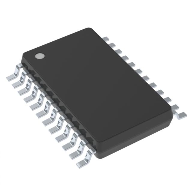
The PI6C2509-133LEX is a PLL Clock Driver IC manufactured by Diodes Incorporated, designed for clock distribution and timing applications requiring a 1:9 input-to-output ratio. This device operates at a maximum frequency of 150MHz with CMOS input and output logic levels, housed in a 24-TSSOP surface mount package.
The PI6C2509-133LEX is classified as obsolete. Identifying equivalent substitute parts is necessary to maintain design continuity, ensure supply chain availability, and support ongoing production requirements for systems utilizing this clock driver architecture.
Substiute Parts
Key Parameters
| Parameter | Value |
|---|---|
| Manufacturer Part Number | PI6C2509-133LEX |
| Manufacturer | Diodes Incorporated |
| Product Category | Clock/Timing - PLL Clock Driver |
| Type | PLL Clock Driver with Bypass |
| Package / Case | 24-TSSOP (0.173", 4.40mm Width) |
| Mounting Type | Surface Mount |
| Input:Output Ratio | 1:9 |
| Maximum Frequency | 150MHz |
| Supply Voltage | 3V ~ 3.6V |
| Operating Temperature Range | 0°C ~ 70°C |
| RoHS Status | ROHS3 Compliant |
| Moisture Sensitivity Level (MSL) | 1 (Unlimited) |
| Product Status | Obsolete |
Substitute Part Grouping Explanation
Substitution of the PI6C2509-133LEX is determined by the following critical parameters that must remain consistent across equivalent parts:
- Package / Case: 24-TSSOP (0.173", 4.40mm Width) — ensures mechanical and electrical compatibility with existing PCB layouts
- Input:Output Ratio: 1:9 — maintains functional equivalence for clock distribution architecture
- Supply Voltage Range: 3V ~ 3.6V — ensures compatibility with power delivery systems
- Mounting Type: Surface Mount — preserves assembly process compatibility
- Number of Circuits: 1 — maintains single-channel clock driver functionality
- PLL with Bypass: Yes — preserves phase-locked loop and bypass mode capabilities
- RoHS Compliance: ROHS3 Compliant — ensures regulatory and environmental compliance
The CDC509PWR from Texas Instruments meets all critical substitution criteria. While the maximum frequency specification differs (125MHz versus 150MHz), this represents a conservative operational envelope suitable for applications within the 125MHz frequency range.
Parameter Comparison
| Parameter | PI6C2509-133LEX (Diodes) | CDC509PWR (Texas Instruments) |
|---|---|---|
| Manufacturer | Diodes Incorporated | Texas Instruments |
| Product Status | Obsolete | Active |
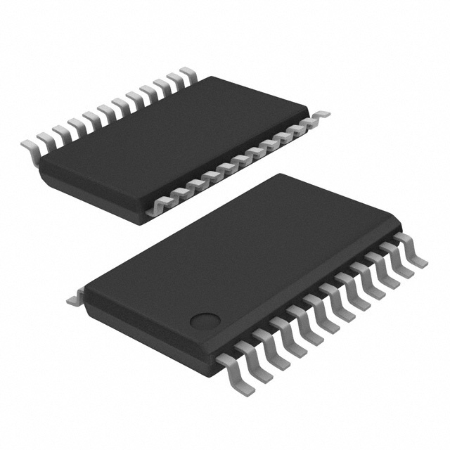
| Package / Case | 24-TSSOP (0.173", 4.40mm Width) | 24-TSSOP (0.173", 4.40mm Width) |
| Input Logic Level | CMOS | LVTTL |
| Output Logic Level | CMOS | LVTTL |
| Input:Output Ratio | 1:9 | 1:9 |
| Maximum Frequency | 150MHz | 125MHz |
| Supply Voltage | 3V ~ 3.6V | 3V ~ 3.6V |
| Operating Temperature Range | 0°C ~ 70°C | 0°C ~ 70°C |
| Number of Circuits | 1 | 1 |
| PLL with Bypass | Yes | Yes |
| Mounting Type | Surface Mount | Surface Mount |
| RoHS Status | ROHS3 Compliant | ROHS3 Compliant |
| Moisture Sensitivity Level (MSL) | 1 (Unlimited) | 1 (Unlimited) |
Engineering Selection Recommendations
The CDC509PWR is the manufacturer-recommended substitute for the obsolete PI6C2509-133LEX. Both devices maintain identical package geometry, pin configuration, and functional architecture, enabling direct replacement in existing designs.
The CDC509PWR offers the advantage of active product status from Texas Instruments, ensuring continued availability and supply chain support. Both parts maintain ROHS3 compliance and identical moisture sensitivity ratings, satisfying regulatory and environmental requirements.
The logic level difference (CMOS input/output on the PI6C2509-133LEX versus LVTTL on the CDC509PWR) is compatible within the specified 3V ~ 3.6V supply voltage range. The reduced maximum frequency specification of the CDC509PWR (125MHz versus 150MHz) does not impact applications operating below 125MHz.
Frequently Asked Questions (FAQ)
Q: Can the CDC509PWR directly replace the PI6C2509-133LEX on existing PCBs?
A: Yes. Both devices use identical 24-TSSOP packaging with matching pin configurations and footprints. No PCB modifications are required.
Q: What is the significance of the logic level difference between CMOS and LVTTL?
A: Both logic families operate within the 3V ~ 3.6V supply voltage range specified for these devices. LVTTL is a subset of CMOS logic compatibility at these voltage levels, making the CDC509PWR functionally compatible with existing signal conditioning circuits.
Q: Does the 125MHz maximum frequency of the CDC509PWR limit its use?
A: The CDC509PWR is suitable for applications operating at or below 125MHz. If your design requires operation above 125MHz, the CDC509PWR is not appropriate for substitution.
Q: Are both parts RoHS compliant?
A: Yes. Both the PI6C2509-133LEX and CDC509PWR are ROHS3 compliant and carry identical Moisture Sensitivity Level (MSL) ratings of 1 (Unlimited).
Q: What is the packaging format for the CDC509PWR?
A: The CDC509PWR is supplied in Tape & Reel (TR) format, standard for high-volume surface mount assembly operations.
Alternative Parts

SJ6012L2TP
Littelfuse Inc.
6 Alternative Parts

JMK107BBJ476MA-RE
Taiyo Yuden
10 Alternative Parts

GMK107BBJ475MA-T
Taiyo Yuden
5 Alternative Parts
SJ6020N2ARP
Littelfuse Inc.
3 Alternative Parts
SJ6025R2ATP
Littelfuse Inc.
4 Alternative Parts

2474-05L
API Delevan Inc.
1 Alternative Parts

4590R-684K
API Delevan Inc.
1 Alternative Parts

CM6560R-334
API Delevan Inc.
1 Alternative Parts

CM6460-104
API Delevan Inc.
1 Alternative Parts

5526-12
API Delevan Inc.
1 Alternative Parts