


Request Quote
(Ships tomorrow)
PI6C2408-1LE Equivalent & Substitute Parts
Part Overview
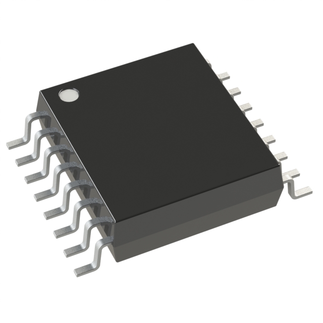
The PI6C2408-1LE is a Zero Delay Buffer IC manufactured by Diodes Incorporated, designed for clock and timing applications requiring high-speed signal distribution. This device operates at a maximum frequency of 140MHz with a 1:8 input-to-output ratio and TTL-level signaling. The part is classified as obsolete, making identification of functionally equivalent alternatives essential for ongoing system support and new design implementations.
Substiute Parts
Key Parameters
| Parameter | Value |
|---|---|
| Manufacturer Part Number | PI6C2408-1LE |
| Manufacturer | Diodes Incorporated |
| Category | Clock/Timing |
| Type | Zero Delay Buffer |
| Package / Case | 16-TSSOP (0.173", 4.40mm Width) |
| Frequency - Max | 140MHz |
| Ratio - Input:Output | 1:8 |
| Voltage - Supply | 3V ~ 3.6V |
| Operating Temperature | 0°C ~ 70°C |
| Input/Output Type | TTL/TTL |
| PLL | Yes with Bypass |
| Mounting Type | Surface Mount |
| Product Status | Obsolete |
| RoHS Status | ROHS3 Compliant |
| MSL Rating | 1 (Unlimited) |
Substitute Part Grouping Explanation
Substitution of the PI6C2408-1LE is determined by the following critical parameters:
Package Compatibility: Both the main part and substitute must use the 16-TSSOP (0.173", 4.40mm Width) surface mount package to ensure PCB-level compatibility without layout modifications.
Supply Voltage Range: The substitute must operate within the 3V to 3.6V supply voltage window to function in existing power distribution networks.
Signal Level Compatibility: The substitute must support TTL or LVTTL input and output signaling to maintain signal integrity with connected logic circuits.
PLL and Bypass Capability: The substitute must include PLL functionality with bypass mode to preserve the zero-delay buffering characteristic and operational flexibility of the original design.
Frequency Performance: The substitute frequency rating must meet or exceed the maximum operating frequency requirement of the application.
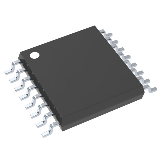
The CDCVF25084PW from Texas Instruments satisfies all substitution criteria while offering enhanced frequency performance (180MHz) and extended operating temperature range (-40°C to 85°C).
Parameter Comparison
| Parameter | PI6C2408-1LE (Main Part) | CDCVF25084PW (Substitute) |
|---|---|---|
| Manufacturer | Diodes Incorporated | Texas Instruments |
| Type | Zero Delay Buffer | PLL Clock Multiplier |
| Package / Case | 16-TSSOP (0.173", 4.40mm Width) | 16-TSSOP (0.173", 4.40mm Width) |
| Frequency - Max | 140MHz | 180MHz |
| Ratio - Input:Output | 1:8 | 2:8 |
| Voltage - Supply | 3V ~ 3.6V | 3V ~ 3.6V |
| Operating Temperature | 0°C ~ 70°C | -40°C ~ 85°C |
| Input/Output Type | TTL/TTL | LVTTL/LVTTL |
| PLL | Yes with Bypass | Yes with Bypass |
| Mounting Type | Surface Mount | Surface Mount |
| Product Status | Obsolete | Active |
| RoHS Status | ROHS3 Compliant | ROHS3 Compliant |
| MSL Rating | 1 (Unlimited) | 1 (Unlimited) |
Engineering Selection Recommendations
The CDCVF25084PW is suitable as a substitute for the PI6C2408-1LE based on the following factors:
Package Equivalence: Both devices use identical 16-TSSOP surface mount packaging, eliminating PCB redesign requirements.
Electrical Compatibility: Supply voltage ranges are identical (3V to 3.6V), and both devices support PLL with bypass functionality. LVTTL signaling is compatible with TTL-level circuits in most applications.
Compliance Status: Both parts are ROHS3 compliant and carry unlimited MSL ratings, meeting current manufacturing and environmental standards.
Product Availability: The CDCVF25084PW is in active production status, ensuring long-term availability and supply chain stability compared to the obsolete PI6C2408-1LE.
Performance Enhancement: The substitute offers higher maximum frequency (180MHz versus 140MHz) and extended operating temperature range (-40°C to 85°C versus 0°C to 70°C), providing design margin for demanding applications.
Frequently Asked Questions (FAQ)
Q: Can the CDCVF25084PW directly replace the PI6C2408-1LE without PCB modifications?
A: Yes. Both devices use the 16-TSSOP package with identical pin spacing and dimensions (0.173", 4.40mm width). No PCB layout changes are required for physical substitution.
Q: Are there signal level compatibility concerns between TTL and LVTTL?
A: LVTTL output levels are compatible with TTL input thresholds in standard logic applications. However, verify that receiving circuits can accept LVTTL voltage levels (typically 0V to 3.3V) if operating at the lower supply voltage boundary.
Q: What is the functional difference between the 1:8 and 2:8 input-to-output ratios?
A: The PI6C2408-1LE provides one input signal distributed to eight outputs. The CDCVF25084PW accepts two input signals and distributes them to eight outputs total. Application requirements determine which ratio is appropriate.
Q: Does the extended operating temperature range of the CDCVF25084PW affect compatibility?
A: The extended range (-40°C to 85°C versus 0°C to 70°C) is a superset of the original specification. Applications operating within the original temperature window will function identically. Applications requiring extended temperature operation benefit from the wider range.
Q: Are both parts RoHS compliant?
A: Yes. Both the PI6C2408-1LE and CDCVF25084PW are ROHS3 compliant with unlimited moisture sensitivity levels, meeting current environmental and manufacturing standards.
Q: What is the significance of the PLL with Bypass feature?
A: This feature allows the device to operate in two modes: PLL mode for frequency multiplication or phase locking, and bypass mode for direct signal buffering. Both devices support this dual-mode operation.
Alternative Parts

SJ6012L2TP
Littelfuse Inc.
6 Alternative Parts

JMK107BBJ476MA-RE
Taiyo Yuden
10 Alternative Parts

GMK107BBJ475MA-T
Taiyo Yuden
5 Alternative Parts
SJ6020N2ARP
Littelfuse Inc.
3 Alternative Parts
SJ6025R2ATP
Littelfuse Inc.
4 Alternative Parts

2474-05L
API Delevan Inc.
1 Alternative Parts

4590R-684K
API Delevan Inc.
1 Alternative Parts

CM6560R-334
API Delevan Inc.
1 Alternative Parts

CM6460-104
API Delevan Inc.
1 Alternative Parts

5526-12
API Delevan Inc.
1 Alternative Parts