


Request Quote
(Ships tomorrow)
PI6C20400SHEX Equivalent & Substitute Parts
Part Overview
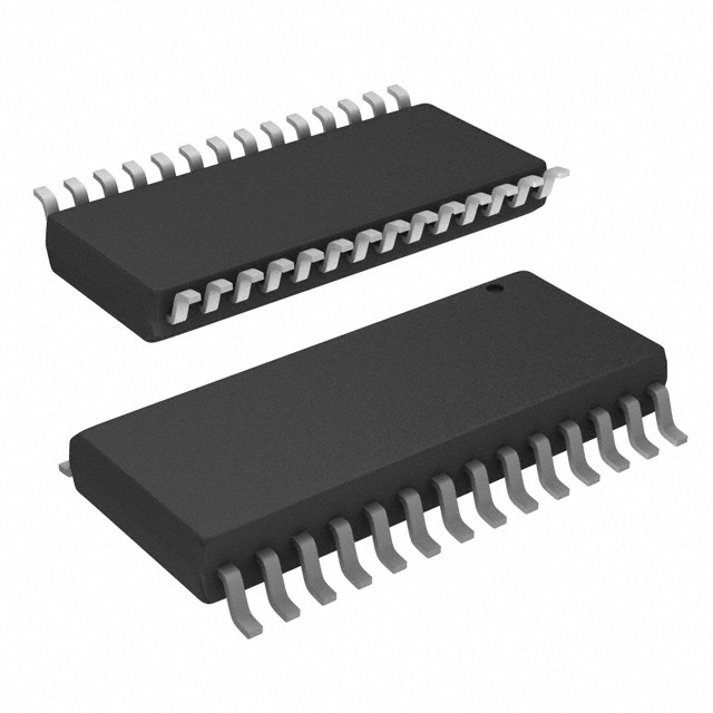
The PI6C20400SHEX is a PCI Express (PCIe) clock buffer IC manufactured by Diodes Incorporated, designed for 1:4 fanout distribution with 100MHz maximum frequency operation. This device features differential input and output capabilities in a 28-SSOP surface mount package. The part is currently classified as obsolete, making identification of functionally equivalent alternatives essential for ongoing system support and new design implementations where legacy compatibility is required.
Substiute Parts
Key Parameters
| Parameter | Value |
|---|---|
| Manufacturer Part Number | PI6C20400SHEX |
| Manufacturer | Diodes Incorporated |
| Category | Clock/Timing |
| Description | IC CLOCK BUFF 1:4 28-SSOP |
| Main Purpose | PCI Express (PCIe) |
| Frequency - Max | 100MHz |
| Ratio - Input:Output | 1:4 |
| Differential - Input:Output | Yes/Yes |
| Voltage - Supply | 3.135V ~ 3.465V |
| Operating Temperature | 0°C ~ 70°C |
| Package / Case | 28-SSOP (0.209", 5.30mm Width) |
| Mounting Type | Surface Mount |
| Product Status | Obsolete |
| RoHS Status | ROHS3 Compliant |
| Moisture Sensitivity Level (MSL) | 1 (Unlimited) |
Substitute Part Grouping Explanation
Substitution of the PI6C20400SHEX is determined by strict alignment of the following critical parameters:
Package Compatibility: Both the main part and substitute must use the 28-SSOP surface mount package with identical physical dimensions (0.209", 5.30mm Width) to ensure PCB layout compatibility without redesign.
Electrical Interface: The substitute must support differential input and differential output configuration to maintain signal integrity in PCIe applications. Input signal type compatibility (LVTTL for the main part) and output signal type must be verified for system-level compatibility.
Functional Specification: The 1:4 fanout ratio (1 input to 4 outputs) is a core functional requirement. The substitute must provide identical or superior frequency capability to support the 100MHz operating specification.
Power Supply: The substitute must operate within the 3.135V ~ 3.465V supply voltage range to ensure compatibility with existing power distribution infrastructure.
Environmental & Compliance: The substitute must maintain ROHS3 compliance and MSL 1 rating to meet manufacturing and storage requirements. Operating temperature range of 0°C ~ 70°C must be supported.
Parameter Comparison
| Parameter | PI6C20400SHEX (Main) | 9DB403DFLF (Substitute) |
|---|---|---|
| Manufacturer | Diodes Incorporated | Renesas Electronics Corporation |
| Category | Clock/Timing | Clock/Timing |
| Main Purpose | PCI Express (PCIe) | PCI Express (PCIe) |
| Frequency - Max | 100MHz | 400MHz |
| Ratio - Input:Output | 1:4 | 1:4 |
| Differential - Input:Output | Yes/Yes | Yes/Yes |
| Input Signal Type | LVTTL | HCSL |
| Output Signal Type | Clock | HCSL, LVDS |
| Voltage - Supply | 3.135V ~ 3.465V | 3.135V ~ 3.465V |
| Operating Temperature | 0°C ~ 70°C | 0°C ~ 70°C |
| Package / Case | 28-SSOP (0.209", 5.30mm Width) | 28-SSOP (0.209", 5.30mm Width) |
| Mounting Type | Surface Mount | Surface Mount |
| Product Status | Obsolete | Active |
| RoHS Status | ROHS3 Compliant | ROHS3 Compliant |
| Moisture Sensitivity Level (MSL) | 1 (Unlimited) | 1 (Unlimited) |
Engineering Selection Recommendations
The 9DB403DFLF from Renesas Electronics Corporation is the qualified substitute for the obsolete PI6C20400SHEX. Both devices share identical package geometry, supply voltage range, operating temperature specifications, and 1:4 fanout ratio. The substitute maintains full ROHS3 compliance and MSL 1 rating, meeting all manufacturing and environmental requirements.
The 9DB403DFLF offers enhanced frequency capability (400MHz maximum versus 100MHz), providing operational margin for PCIe clock distribution applications. The device is currently in active production status, ensuring long-term availability and supply chain stability compared to the obsolete main part.
Signal interface differences exist between the devices: the main part specifies LVTTL input with clock output, while the substitute provides HCSL input with HCSL and LVDS output options. These differences require system-level signal integrity analysis to confirm compatibility with existing driver and receiver circuits in the target application.
Frequently Asked Questions (FAQ)
Q: Can the 9DB403DFLF directly replace the PI6C20400SHEX without PCB modifications?
A: The 9DB403DFLF uses the identical 28-SSOP package with matching pin pitch and physical dimensions, enabling direct PCB footprint compatibility. However, signal interface differences (LVTTL input versus HCSL input, and output signal type variations) require circuit-level verification to confirm functional compatibility with upstream and downstream components.
Q: What is the significance of the higher 400MHz frequency rating on the substitute?
A: The 9DB403DFLF's 400MHz maximum frequency specification exceeds the PI6C20400SHEX's 100MHz rating. This provides operational margin and future-proofs the design for higher-speed PCIe applications. The substitute remains fully compatible with 100MHz operation, as it can operate at frequencies below its maximum rating.
Q: Are there any supply chain or availability advantages to using the substitute?
A: The 9DB403DFLF is classified as active product status with current manufacturing and distribution support from Renesas Electronics Corporation. The PI6C20400SHEX is obsolete, making the substitute the only viable long-term sourcing option for new designs or system refreshes.
Q: How do the input signal types (LVTTL versus HCSL) affect substitution feasibility?
A: Input signal type compatibility depends on the clock source driving the buffer IC. LVTTL and HCSL are distinct signaling standards with different voltage levels and impedance characteristics. The system design must confirm that the clock source can drive HCSL input levels, or signal conditioning may be required.
Q: What compliance certifications are maintained across both parts?
A: Both the PI6C20400SHEX and 9DB403DFLF maintain ROHS3 compliance and MSL 1 (Unlimited) moisture sensitivity rating. Both devices operate within the identical 3.135V ~ 3.465V supply voltage range and 0°C ~ 70°C temperature specification, ensuring regulatory and environmental compatibility.
Alternative Parts

SJ6012L2TP
Littelfuse Inc.
6 Alternative Parts

JMK107BBJ476MA-RE
Taiyo Yuden
10 Alternative Parts

GMK107BBJ475MA-T
Taiyo Yuden
5 Alternative Parts
SJ6020N2ARP
Littelfuse Inc.
3 Alternative Parts
SJ6025R2ATP
Littelfuse Inc.
4 Alternative Parts

2474-05L
API Delevan Inc.
1 Alternative Parts

4590R-684K
API Delevan Inc.
1 Alternative Parts

CM6560R-334
API Delevan Inc.
1 Alternative Parts

CM6460-104
API Delevan Inc.
1 Alternative Parts

5526-12
API Delevan Inc.
1 Alternative Parts