


Request Quote
(Ships tomorrow)
PI49FCT3802LEX Equivalent & Substitute Parts
Part Overview
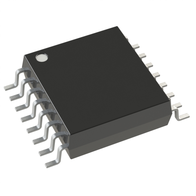
The PI49FCT3802LEX is a Clock Fanout Buffer (Distribution) IC manufactured by Diodes Incorporated, designed for 1:5 clock distribution at frequencies up to 156 MHz. This device operates with CMOS/TTL input and output compatibility, housed in a 16-TSSOP surface mount package. The part is currently classified as obsolete, making identification of suitable substitute components essential for ongoing system support and new design implementations.
Substiute Parts
Key Parameters
| Parameter | Value |
|---|---|
| Manufacturer Part Number | PI49FCT3802LEX |
| Manufacturer | Diodes Incorporated |
| Category | Clock/Timing |
| Type | Fanout Buffer (Distribution) |
| Ratio - Input:Output | 1:5 |
| Frequency - Max | 156 MHz |
| Input/Output Logic | CMOS, TTL |
| Voltage - Supply | 3V ~ 3.6V |
| Operating Temperature | 0°C ~ 70°C |
| Package / Case | 16-TSSOP (0.173", 4.40mm Width) |
| Mounting Type | Surface Mount |
| Product Status | Obsolete |
| RoHS Status | ROHS3 Compliant |
| Moisture Sensitivity Level (MSL) | 1 (Unlimited) |
Substitute Part Grouping Explanation
Substitution of the PI49FCT3802LEX is determined by the following critical parameters that must remain compatible:
Mandatory Compatibility Parameters:
- Package / Case: 16-TSSOP (0.173", 4.40mm Width) — ensures PCB footprint compatibility
- Mounting Type: Surface Mount — maintains assembly process compatibility
- Input/Output Logic: CMOS, TTL — preserves signal interface compatibility
- Voltage - Supply: 3V ~ 3.6V — ensures power supply compatibility
- Frequency - Max: 156 MHz or higher — maintains or exceeds timing performance
- Operating Temperature: 0°C ~ 70°C — meets or exceeds thermal operating range
Functional Parameters:
- Type: Fanout Buffer (Distribution) — maintains clock distribution functionality
- Number of Circuits: 1 — preserves single-channel architecture
The PI49FCT3802LEX operates as a 1:5 fanout buffer. Substitute parts may have different output ratios (such as 1:7) provided all mandatory compatibility parameters are met. The higher output ratio does not prevent substitution, as the device can be configured to use only the required number of outputs.
Parameter Comparison
| Parameter | PI49FCT3802LEX (Main Part) | PI49FCT3803LEX (Substitute) | Compatibility |
|---|---|---|---|
| Manufacturer Part Number | PI49FCT3802LEX | PI49FCT3803LEX | Different part numbers |
| Manufacturer | Diodes Incorporated | Diodes Incorporated | Same manufacturer |
| Type | Fanout Buffer (Distribution) | Fanout Buffer (Distribution) | Compatible |
| Ratio - Input:Output | 1:5 | 1:7 | Different ratio; substitute has higher output count |
| Frequency - Max | 156 MHz | 156 MHz | Compatible |
| Input/Output Logic | CMOS, TTL | CMOS, TTL | Compatible |
| Voltage - Supply | 3V ~ 3.6V | 3V ~ 3.6V | Compatible |
| Operating Temperature | 0°C ~ 70°C | 0°C ~ 70°C | Compatible |
| Package / Case | 16-TSSOP (0.173", 4.40mm Width) | 16-TSSOP (0.173", 4.40mm Width) | Compatible |
| Mounting Type | Surface Mount | Surface Mount | Compatible |
| Product Status | Obsolete | Active | Substitute is actively manufactured |
| RoHS Status | ROHS3 Compliant | ROHS3 Compliant | Compatible |
| Moisture Sensitivity Level (MSL) | 1 (Unlimited) | 1 (Unlimited) | Compatible |
Engineering Selection Recommendations
The PI49FCT3803LEX is a direct substitute for the obsolete PI49FCT3802LEX based on the following engineering criteria:
Product Status Alignment: The PI49FCT3803LEX holds Active product status, ensuring continued manufacturing availability, supply chain reliability, and long-term support compared to the obsolete PI49FCT3802LEX.
Compliance & Certification: Both parts maintain identical ROHS3 compliance and REACH unaffected status, ensuring regulatory compatibility in existing and new applications.
Electrical & Mechanical Compatibility: The substitute part maintains identical supply voltage (3V ~ 3.6V), operating temperature range (0°C ~ 70°C), maximum frequency (156 MHz), logic compatibility (CMOS/TTL), and physical package specifications (16-TSSOP surface mount).
Functional Consideration: The PI49FCT3803LEX provides 1:7 output distribution compared to the 1:5 configuration of the PI49FCT3802LEX. This higher output count does not prevent substitution, as designs requiring only 5 outputs can utilize the available outputs while leaving additional outputs unused or unconnected.
Frequently Asked Questions (FAQ)
Q: Can the PI49FCT3803LEX directly replace the PI49FCT3802LEX on existing PCBs?
A: Yes. Both parts use identical 16-TSSOP surface mount packaging with the same footprint dimensions (0.173", 4.40mm width). No PCB redesign is required.
Q: What is the difference between the 1:5 and 1:7 output ratios?
A: The PI49FCT3802LEX distributes one input clock signal to 5 output channels. The PI49FCT3803LEX distributes one input clock signal to 7 output channels. If your design requires only 5 outputs, the additional 2 outputs on the PI49FCT3803LEX can remain unconnected without affecting performance.
Q: Are the electrical specifications identical between these parts?
A: Yes. Both parts operate at 3V ~ 3.6V supply voltage, support 0°C ~ 70°C operating temperature, achieve 156 MHz maximum frequency, and provide CMOS/TTL input and output compatibility.
Q: Why is the PI49FCT3802LEX listed as obsolete?
A: The PI49FCT3802LEX has been discontinued by the manufacturer. The PI49FCT3803LEX remains in active production and is the recommended substitute for new designs and ongoing system support.
Q: Are there any compliance differences between these parts?
A: No. Both parts maintain ROHS3 compliance, REACH unaffected status, and identical moisture sensitivity level (MSL 1 - Unlimited).
Q: Can I use the PI49FCT3803LEX in applications originally designed for the PI49FCT3802LEX?
A: Yes, provided your application can accommodate the higher output count. The electrical performance, timing characteristics, and physical package are fully compatible.
Alternative Parts

SJ6012L2TP
Littelfuse Inc.
6 Alternative Parts

JMK107BBJ476MA-RE
Taiyo Yuden
10 Alternative Parts

GMK107BBJ475MA-T
Taiyo Yuden
5 Alternative Parts
SJ6020N2ARP
Littelfuse Inc.
3 Alternative Parts
SJ6025R2ATP
Littelfuse Inc.
4 Alternative Parts

2474-05L
API Delevan Inc.
1 Alternative Parts

4590R-684K
API Delevan Inc.
1 Alternative Parts

CM6560R-334
API Delevan Inc.
1 Alternative Parts

CM6460-104
API Delevan Inc.
1 Alternative Parts

5526-12
API Delevan Inc.
1 Alternative Parts