


Request Quote
(Ships tomorrow)
PDTC114YQBZ Equivalent & Substitute Parts
Part Overview
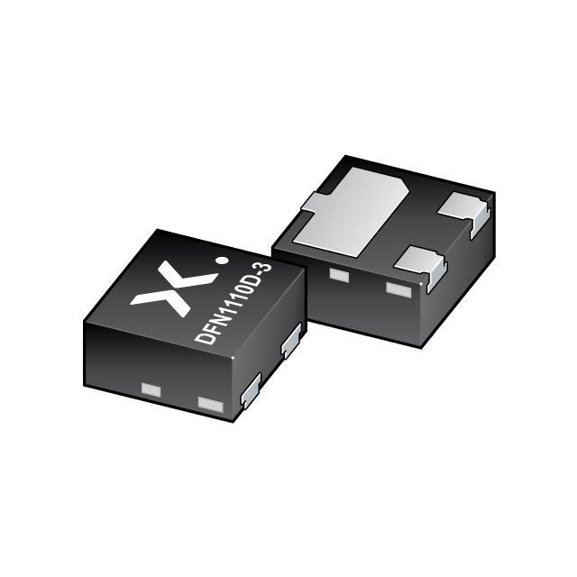
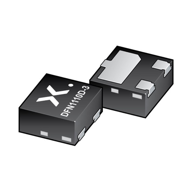
The PDTC114YQBZ is a pre-biased PNP bipolar junction transistor manufactured by Nexperia USA Inc. in a 3-XDFN surface mount package with wettable flank. This device integrates internal base resistors (R1: 10 kOhms, R2: 47 kOhms) for simplified circuit design and reduced component count. The part is rated for 50 V collector-emitter breakdown voltage and 100 mA maximum collector current with 340 mW power dissipation capability.
The PDTC114YQBZ is currently listed as obsolete. Identifying equivalent substitute parts is necessary to maintain design continuity and ensure availability for new production runs, repairs, and ongoing system support.
Substiute Parts
Key Parameters
| Parameter | Value | Unit |
|---|---|---|
| Transistor Type | PNP - Pre-Biased | — |
| Current - Collector (Ic) Max | 100 | mA |
| Voltage - Collector Emitter Breakdown (Max) | 50 | V |
| Resistor - Base (R1) | 10 | kOhms |
| Resistor - Emitter Base (R2) | 47 | kOhms |
| DC Current Gain (hFE) Min @ Ic, Vce | 100 @ 5mA, 5V | — |
| Vce Saturation (Max) @ Ib, Ic | 100 | mV @ 250µA, 5mA |
| Current - Collector Cutoff (Max) | 100 | nA |
| Frequency - Transition | 180 | MHz |
| Power - Max | 340 | mW |
| Package / Case | 3-XDFN Exposed Pad | — |
| Mounting Type | Surface Mount, Wettable Flank | — |
| RoHS Status | ROHS3 Compliant | — |
| Moisture Sensitivity Level (MSL) | 3 (168 Hours) | — |
Substitute Part Grouping Explanation
Substitution of the PDTC114YQBZ is constrained by the following critical parameters:
Transistor Polarity: The main part is a PNP pre-biased transistor. Direct substitutes must maintain PNP polarity to preserve circuit functionality and signal flow characteristics.
Electrical Ratings: Substitute parts must meet or exceed the following specifications:
- Maximum collector current: 100 mA
- Collector-emitter breakdown voltage: 50 V
- Power dissipation: 340 mW
- DC current gain (hFE): minimum 100 @ 5mA, 5V
- Saturation voltage: 100 mV maximum @ 250µA, 5mA
Internal Resistor Configuration: The integrated base resistor (R1: 10 kOhms) and emitter-base resistor (R2: 47 kOhms) are functional elements. Substitutes must incorporate identical resistor values to maintain biasing characteristics and circuit behavior.
Package Compatibility: The 3-XDFN exposed pad package with wettable flank is the specified form factor. Substitutes must use the identical package designation (DFN1110D-3) to ensure PCB footprint compatibility and manufacturing process alignment.
Compliance Requirements: Substitutes must maintain ROHS3 compliance and REACH unaffected status to satisfy regulatory and supply chain requirements.
Parameter Comparison
| Parameter | PDTC114YQBZ (Main Part) | PDTC114YQB-QZ (Substitute) |
|---|---|---|
| Manufacturer | Nexperia USA Inc. | Nexperia USA Inc. |
| Transistor Type | PNP - Pre-Biased | NPN - Pre-Biased |
| Current - Collector (Ic) Max | 100 mA | 100 mA |
| Voltage - Collector Emitter Breakdown (Max) | 50 V | 50 V |
| Resistor - Base (R1) | 10 kOhms | 10 kOhms |
| Resistor - Emitter Base (R2) | 47 kOhms | 47 kOhms |
| DC Current Gain (hFE) Min @ Ic, Vce | 100 @ 5mA, 5V | 100 @ 5mA, 5V |
| Vce Saturation (Max) @ Ib, Ic | 100 mV @ 250µA, 5mA | 100 mV @ 250µA, 5mA |
| Current - Collector Cutoff (Max) | 100 nA | 100 nA |
| Frequency - Transition | 180 MHz | 230 MHz |
| Power - Max | 340 mW | 340 mW |
| Package / Case | 3-XDFN Exposed Pad | 3-XDFN Exposed Pad |
| Mounting Type | Surface Mount, Wettable Flank | Surface Mount, Wettable Flank |
| RoHS Status | ROHS3 Compliant | ROHS3 Compliant |
| Moisture Sensitivity Level (MSL) | 3 (168 Hours) | 1 (Unlimited) |
| Product Status | Obsolete | Active |
| Grade | — | Automotive |
| Qualification | — | AEC-Q101 |
Engineering Selection Recommendations
The PDTC114YQB-QZ is listed as the manufacturer-recommended substitute for the obsolete PDTC114YQBZ. Both devices are manufactured by Nexperia USA Inc. and share identical electrical ratings for collector current, breakdown voltage, power dissipation, current gain, and saturation characteristics. Both maintain ROHS3 compliance and REACH unaffected status.
The PDTC114YQB-QZ differs from the main part in the following aspects:
Transistor Polarity: The substitute is an NPN pre-biased transistor, whereas the main part is PNP. This polarity difference requires circuit redesign and is not a direct pin-compatible substitution. The NPN variant is suitable only for applications where PNP-to-NPN conversion is acceptable within the system architecture.
Product Status: The PDTC114YQB-QZ is active and in production, ensuring long-term availability and supply chain stability compared to the obsolete PDTC114YQBZ.
Moisture Sensitivity: The substitute features MSL 1 (unlimited moisture exposure tolerance) compared to MSL 3 (168 hours) for the main part. This provides improved handling flexibility during manufacturing and storage.
Automotive Qualification: The PDTC114YQB-QZ carries AEC-Q101 automotive qualification and automotive grade designation, indicating suitability for automotive applications with enhanced reliability requirements.
Transition Frequency: The substitute exhibits 230 MHz transition frequency compared to 180 MHz for the main part, providing higher frequency performance capability.
Frequently Asked Questions (FAQ)
Q: Can the PDTC114YQB-QZ be used as a direct replacement for the PDTC114YQBZ?
A: The PDTC114YQB-QZ is not a direct pin-compatible replacement. While both devices share identical package form factor (3-XDFN), identical electrical ratings for current and voltage, and identical internal resistor values, the PDTC114YQB-QZ is an NPN transistor whereas the PDTC114YQBZ is a PNP transistor. Circuit redesign is required to accommodate the polarity difference.
Q: What are the key electrical parameters that must match between the main part and a substitute?
A: Critical matching parameters include maximum collector current (100 mA), collector-emitter breakdown voltage (50 V), internal base resistor value (10 kOhms), internal emitter-base resistor value (47 kOhms), DC current gain minimum (100 @ 5mA, 5V), and saturation voltage (100 mV @ 250µA, 5mA). Deviations in these parameters affect circuit biasing, switching speed, and overall system performance.
Q: Are there package compatibility considerations between these parts?
A: Both the PDTC114YQBZ and PDTC114YQB-QZ use the identical 3-XDFN exposed pad package (DFN1110D-3) with wettable flank. PCB footprints and reflow soldering processes are compatible. However, the transistor polarity difference requires circuit-level modifications independent of package considerations.
Q: What is the significance of the MSL rating difference?
A: The PDTC114YQBZ carries MSL 3 (168 hours), limiting moisture exposure before soldering. The PDTC114YQB-QZ carries MSL 1 (unlimited), allowing indefinite storage without moisture bake-out requirements. This difference affects component handling procedures and storage conditions but does not impact electrical performance.
Q: Why is the PDTC114YQB-QZ listed as automotive grade?
A: The PDTC114YQB-QZ carries AEC-Q101 automotive qualification, indicating compliance with automotive industry reliability and quality standards. This designation reflects enhanced testing, traceability, and performance validation suitable for automotive applications. The main part carries no automotive designation.
Q: How does the transition frequency difference affect circuit performance?
A: The PDTC114YQB-QZ exhibits 230 MHz transition frequency compared to 180 MHz for the main part. This higher frequency capability provides improved switching speed and bandwidth performance. For applications operating below 180 MHz, this difference is not functionally significant. For higher-frequency applications, the substitute offers enhanced performance margin.
Alternative Parts

SJ6012L2TP
Littelfuse Inc.
6 Alternative Parts

JMK107BBJ476MA-RE
Taiyo Yuden
10 Alternative Parts

GMK107BBJ475MA-T
Taiyo Yuden
5 Alternative Parts
SJ6020N2ARP
Littelfuse Inc.
3 Alternative Parts
SJ6025R2ATP
Littelfuse Inc.
4 Alternative Parts

2474-05L
API Delevan Inc.
1 Alternative Parts

4590R-684K
API Delevan Inc.
1 Alternative Parts

CM6560R-334
API Delevan Inc.
1 Alternative Parts

CM6460-104
API Delevan Inc.
1 Alternative Parts

5526-12
API Delevan Inc.
1 Alternative Parts