


Request Quote
(Ships tomorrow)
PCK351DB,112 Equivalent & Substitute Parts
Part Overview
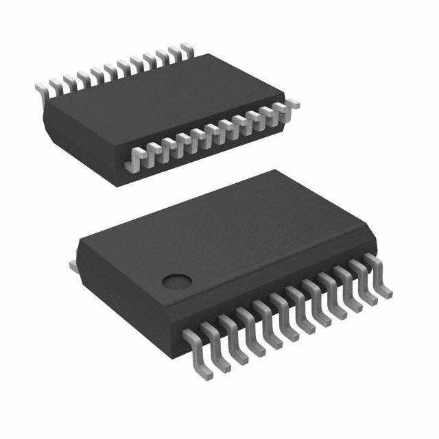
The PCK351DB,112 is a Clock Fanout Buffer (Distribution) IC manufactured by NXP USA Inc., designed for 1:10 clock distribution at 125 MHz with LVTTL input/output levels. This part operates across a -40°C to 85°C temperature range and is housed in a 24-SSOP surface mount package. The PCK351DB,112 is classified as obsolete, making equivalent substitute parts necessary for new designs and ongoing production requirements.
Substiute Parts
Key Parameters
| Parameter | Value |
|---|---|
| Manufacturer | NXP USA Inc. |
| Part Number | PCK351DB,112 |
| Product Category | Clock/Timing - Fanout Buffer (Distribution) |
| Type | Fanout Buffer (Distribution) |
| Number of Circuits | 1 |
| Ratio - Input:Output | 1:10 |
| Input Logic Level | LVTTL |
| Output Logic Level | LVTTL |
| Frequency - Max | 125 MHz |
| Voltage - Supply | 3V ~ 3.6V |
| Operating Temperature | -40°C ~ 85°C |
| Mounting Type | Surface Mount |
| Package / Case | 24-SSOP (0.209", 5.30mm Width) |
| RoHS Status | ROHS3 Compliant |
| Product Status | Obsolete |
Substitute Part Grouping Explanation
Substitution of the PCK351DB,112 is determined by the following critical parameters:
Electrical Compatibility Requirements:
- Input/Output Logic Levels: LVTTL (mandatory match)
- Supply Voltage Range: 3V ~ 3.6V (mandatory match)
- Input:Output Ratio: 1:10 (mandatory match)
- Number of Circuits: 1 (mandatory match)
- Package Type: 24-SSOP (mandatory match)
Acceptable Variations:
- Maximum Frequency: Substitute parts operating at 100 MHz are acceptable for applications requiring ≤100 MHz operation
- Operating Temperature Range: Substitute parts with extended or different temperature ranges are acceptable if the application requirements fall within the substitute's specified range
- Output Configuration: CDC351 series parts with TRI-State output capability are functionally compatible with standard LVTTL output
- Packaging Format: Tube and Tape & Reel (TR) packaging are interchangeable for the same die
Texas Instruments CDC2351 and CDC351 series parts meet all mandatory electrical and mechanical compatibility criteria with the PCK351DB,112.
Parameter Comparison
| Parameter | PCK351DB,112 | CDC2351DB | CDC2351DBR | CDC2351MDBREP | CDC2351QDB | CDC2351QDBG4 | CDC2351QDBR | CDC351DB | CDC351DBR | CDC351IDB | CDC351IDBR |
|---|---|---|---|---|---|---|---|---|---|---|---|
| Manufacturer | NXP USA Inc. | Texas Instruments | Texas Instruments | Texas Instruments | Texas Instruments | Texas Instruments | Texas Instruments | Texas Instruments | Texas Instruments | Texas Instruments | Texas Instruments |
| Type | Fanout Buffer | Fanout Buffer | Fanout Buffer | Fanout Buffer | Fanout Buffer | Fanout Buffer | Fanout Buffer | Fanout Buffer | Fanout Buffer | Fanout Buffer | Fanout Buffer |
| Ratio - Input:Output | 1:10 | 1:10 | 1:10 | 1:10 | 1:10 | 1:10 | 1:10 | 1:10 | 1:10 | 1:10 | 1:10 |
| Input Logic Level | LVTTL | LVTTL | LVTTL | LVTTL | LVTTL | LVTTL | LVTTL | LVTTL | LVTTL | LVTTL | LVTTL |
| Output Logic Level | LVTTL | LVTTL | LVTTL | LVTTL | LVTTL | LVTTL | LVTTL | LVTTL, TRI-State | LVTTL, TRI-State | LVTTL, TRI-State | LVTTL, TRI-State |
| Frequency - Max | 125 MHz | 100 MHz | 100 MHz | 100 MHz | 100 MHz | 100 MHz | 100 MHz | 100 MHz | 100 MHz | 100 MHz | 100 MHz |
| Voltage - Supply | 3V ~ 3.6V | 3V ~ 3.6V | 3V ~ 3.6V | 3V ~ 3.6V | 3V ~ 3.6V | 3V ~ 3.6V | 3V ~ 3.6V | 3V ~ 3.6V | 3V ~ 3.6V | 3V ~ 3.6V | 3V ~ 3.6V |
| Operating Temperature | -40°C ~ 85°C | 0°C ~ 70°C | 0°C ~ 70°C | -55°C ~ 125°C | -40°C ~ 125°C | -40°C ~ 125°C | -40°C ~ 125°C | 0°C ~ 70°C | 0°C ~ 70°C | -40°C ~ 85°C | -40°C ~ 85°C |
| Package / Case | 24-SSOP | 24-SSOP | 24-SSOP | 24-SSOP | 24-SSOP | 24-SSOP | 24-SSOP | 24-SSOP | 24-SSOP | 24-SSOP | 24-SSOP |
| Mounting Type | Surface Mount | Surface Mount | Surface Mount | Surface Mount | Surface Mount | Surface Mount | Surface Mount | Surface Mount | Surface Mount | Surface Mount | Surface Mount |
| RoHS Status | ROHS3 Compliant | ROHS3 Compliant | ROHS3 Compliant | ROHS3 Compliant | ROHS3 Compliant | ROHS3 Compliant | ROHS3 Compliant | ROHS3 Compliant | ROHS3 Compliant | ROHS3 Compliant | ROHS3 Compliant |
| Product Status | Obsolete | Active | Active | Active | Active | Discontinued | Active | Active | Active | Active | Active |
Engineering Selection Recommendations
Primary Substitutes (Recommended for New Designs):
CDC2351QDB and CDC2351QDBR are the preferred substitutes. Both parts are active products with automotive-grade qualification (AEC-Q100) and extended operating temperature range (-40°C to 125°C), which exceeds the original PCK351DB,112 specification. These parts provide superior temperature coverage for demanding applications.
CDC351IDB and CDC351IDBR are suitable alternatives with operating temperature range of -40°C to 85°C, matching the original part's thermal specification. These parts include TRI-State output capability, providing additional design flexibility.
Secondary Substitutes (For Specific Applications):
CDC2351DB and CDC2351DBR operate within 0°C to 70°C temperature range. These are acceptable only for applications where operating temperature remains within this narrower window.
CDC351DB and CDC351DBR also operate within 0°C to 70°C range and include TRI-State output. Selection depends on application temperature requirements.
CDC2351MDBREP supports extended military-grade temperature range (-55°C to 125°C) with MSL Level 2 moisture sensitivity. This variant is suitable for extreme environment applications.
Frequency Consideration:
All substitute parts operate at 100 MHz maximum frequency, which is lower than the original 125 MHz specification. Substitutes are suitable only for applications requiring ≤100 MHz operation. Applications requiring 125 MHz operation cannot use these substitutes.
Frequently Asked Questions (FAQ)
Q: Can CDC2351 series parts directly replace PCK351DB,112 in existing designs?
A: Yes, provided the application operates at ≤100 MHz. All CDC2351 variants maintain identical 1:10 ratio, LVTTL input/output levels, 3V-3.6V supply voltage, and 24-SSOP package. The primary difference is maximum frequency (100 MHz vs. 125 MHz) and operating temperature ranges. Select the variant matching your temperature requirements.
Q: What is the difference between CDC2351DB and CDC2351DBR?
A: Both parts are electrically identical. CDC2351DB is packaged in Tube format, while CDC2351DBR is packaged in Tape & Reel (TR) format. Selection depends on assembly process requirements and volume. Tape & Reel packaging is standard for automated pick-and-place assembly.
Q: Why do CDC351 parts have TRI-State output while CDC2351 parts do not?
A: CDC351 and CDC2351 are different product lines within Texas Instruments' clock buffer portfolio. CDC351 includes TRI-State output control, providing additional design flexibility for bus-sharing applications. CDC2351 provides standard LVTTL output. Both are functionally compatible with PCK351DB,112 for standard clock distribution applications.
Q: Is CDC2351QDBG4 suitable for production use?
A: CDC2351QDBG4 is discontinued at DiGi Electronics, though inventory remains available. For new production designs, select active product variants such as CDC2351QDB, CDC2351QDBR, CDC351IDB, or CDC351IDBR to ensure long-term supply availability.
Q: Can I use CDC2351MDBREP in commercial applications?
A: CDC2351MDBREP is specified for military-grade temperature range (-55°C to 125°C) and carries MSL Level 2 moisture sensitivity. While electrically compatible, this part is optimized for military and aerospace applications. For standard commercial applications, CDC2351QDB or CDC351IDB variants are more appropriate.
Q: What is the impact of operating temperature range differences?
A: The original PCK351DB,112 operates -40°C to 85°C. CDC2351QDB/QDBR extend this to -40°C to 125°C, providing additional margin for high-temperature environments. CDC2351DB/DBR limit operation to 0°C to 70°C. Select the substitute variant whose temperature range encompasses your application's operating conditions.
Q: Are all substitutes ROHS3 compliant?
A: Yes. All listed substitute parts maintain ROHS3 compliance, matching the original PCK351DB,112 specification. All parts are also REACH unaffected and carry EAR99 ECCN classification.
Alternative Parts

SJ6012L2TP
Littelfuse Inc.
6 Alternative Parts

JMK107BBJ476MA-RE
Taiyo Yuden
10 Alternative Parts

GMK107BBJ475MA-T
Taiyo Yuden
5 Alternative Parts
SJ6020N2ARP
Littelfuse Inc.
3 Alternative Parts
SJ6025R2ATP
Littelfuse Inc.
4 Alternative Parts

2474-05L
API Delevan Inc.
1 Alternative Parts

4590R-684K
API Delevan Inc.
1 Alternative Parts

CM6560R-334
API Delevan Inc.
1 Alternative Parts

CM6460-104
API Delevan Inc.
1 Alternative Parts

5526-12
API Delevan Inc.
1 Alternative Parts