


Request Quote
(Ships tomorrow)
PBSS4420D,115 Equivalent & Substitute Parts
Part Overview
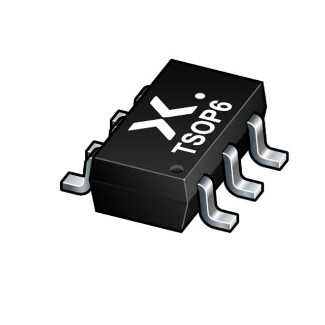
The PBSS4420D,115 is an NPN bipolar junction transistor manufactured by Nexperia USA Inc., designed for surface mount applications in the 6-TSOP package. This component operates at a maximum collector current of 4 A with a collector-emitter breakdown voltage of 20 V and a maximum power dissipation of 1.1 W. The device is qualified to AEC-Q100 automotive standards and maintains active product status with 880 units currently in stock.
Substitute parts become necessary when the primary component experiences supply constraints, extended lead times, or when design requirements permit operation within alternative electrical specifications. The NSS20201MR6T1G represents a viable alternative, though it operates at reduced maximum collector current and power ratings while offering enhanced frequency performance.
Substiute Parts
Key Parameters
| Parameter | PBSS4420D,115 |
|---|---|
| Transistor Type | NPN |
| Voltage - Collector Emitter Breakdown (Max) | 20 V |
| Current - Collector (Ic) (Max) | 4 A |
| Power - Max | 1.1 W |
| Frequency - Transition | 100 MHz |
| DC Current Gain (hFE) (Min) | 250 @ 2A, 2V |
| Vce Saturation (Max) | 1.1 V @ 400mA, 4A |
| Package / Case | SC-74, SOT-457 (6-TSOP) |
| Operating Temperature (Max) | 150°C (TJ) |
| Product Status | Active |
| Grade | Automotive (AEC-Q100) |
Substitute Part Grouping Explanation
Substitution compatibility for the PBSS4420D,115 is determined by the following critical electrical and mechanical parameters:
Mandatory Matching Parameters:
- Transistor Type: NPN configuration
- Voltage - Collector Emitter Breakdown: 20 V minimum
- Package / Case: 6-TSOP surface mount form factor
- Mounting Type: Surface Mount
Allowable Variation Parameters:
- Current - Collector (Ic) (Max): Substitute must support minimum 4 A or lower (derated applications acceptable)
- Power - Max: Substitute must support minimum 1.1 W or lower (derated applications acceptable)
- Frequency - Transition: Substitute may exceed 100 MHz
- DC Current Gain (hFE): Substitute may vary from 250 @ 2A, 2V specification
- Vce Saturation: Substitute may vary from 1.1 V specification
- Operating Temperature: Substitute must support minimum 150°C (TJ)
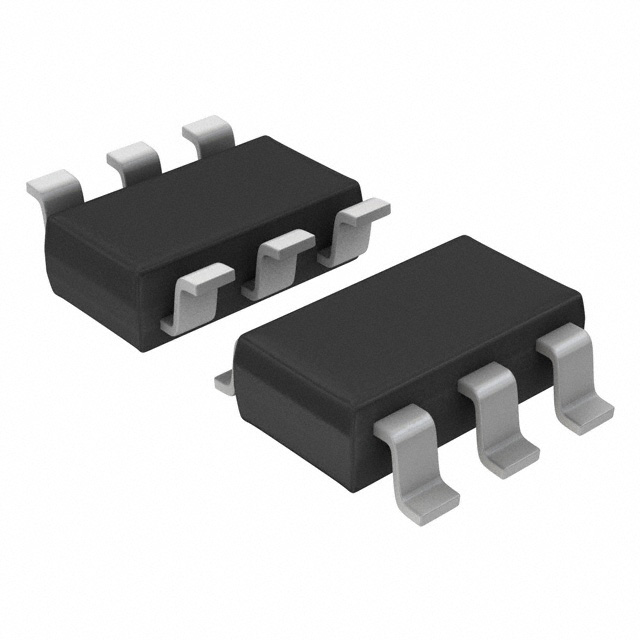
The NSS20201MR6T1G qualifies as a substitute based on matching transistor type, voltage rating, and package configuration. However, the reduced maximum collector current (2 A versus 4 A) and power dissipation (460 mW versus 1.1 W) restrict its application to circuits designed for lower current operation.
Parameter Comparison
| Parameter | PBSS4420D,115 | NSS20201MR6T1G | Compatibility Notes |
|---|---|---|---|
| Transistor Type | NPN | NPN | Matched |
| Voltage - Collector Emitter Breakdown (Max) | 20 V | 20 V | Matched |
| Current - Collector (Ic) (Max) | 4 A | 2 A | Substitute rated lower; suitable for derated applications |
| Power - Max | 1.1 W | 460 mW | Substitute rated lower; suitable for derated applications |
| Frequency - Transition | 100 MHz | 200 MHz | Substitute exceeds specification |
| DC Current Gain (hFE) (Min) | 250 @ 2A, 2V | 200 @ 1A, 5V | Measured at different operating points |
| Vce Saturation (Max) | 1.1 V @ 400mA, 4A | 150 mV @ 100mA, 1A | Measured at different operating points |
| Current - Collector Cutoff (Max) | 100 nA | 100 nA | Matched |
| Package / Case | SC-74, SOT-457 (6-TSOP) | SOT-23-6 Thin, TSOT-23-6 (6-TSOP) | Matched package family; pin-compatible |
| Operating Temperature (Max) | 150°C (TJ) | 150°C (TJ) | Matched |
| Mounting Type | Surface Mount | Surface Mount | Matched |
| Product Status | Active | Obsolete | Primary part maintains active status |
| RoHS Status | ROHS3 Compliant | ROHS3 Compliant | Matched |
| Moisture Sensitivity Level (MSL) | 1 (Unlimited) | 1 (Unlimited) | Matched |
Engineering Selection Recommendations
Primary Component Selection: The PBSS4420D,115 is the recommended choice for new designs and production applications. This component maintains active product status, ensuring long-term availability and supply chain stability. Automotive-grade qualification (AEC-Q100) and ROHS3 compliance support deployment in regulated environments. The 4 A maximum collector current and 1.1 W power dissipation provide design margin for applications requiring higher current handling or thermal performance.
Substitute Component Consideration: The NSS20201MR6T1G may be selected only when circuit design specifications permit operation at reduced maximum collector current (2 A) and power dissipation (460 mW). This substitute carries obsolete product status, indicating discontinued manufacturing and potential future supply unavailability. Selection of this substitute introduces supply chain risk and should be limited to legacy system maintenance or temporary supply mitigation.
Both components satisfy the mandatory electrical and mechanical compatibility criteria: NPN transistor type, 20 V collector-emitter breakdown voltage, and 6-TSOP surface mount package. Compliance certifications (ROHS3, unlimited MSL) are equivalent between both parts.
Frequently Asked Questions (FAQ)
Q: Can the NSS20201MR6T1G directly replace the PBSS4420D,115 in all applications?
A: No. The NSS20201MR6T1G is suitable only for applications designed to operate at maximum collector currents of 2 A or lower and power dissipation of 460 mW or lower. Circuits requiring the full 4 A current capability or 1.1 W power handling of the PBSS4420D,115 will not function correctly with the substitute part.
Q: Are the 6-TSOP packages of both parts physically and electrically identical?
A: Both parts use 6-TSOP surface mount packages and are pin-compatible. The PBSS4420D,115 uses SC-74 or SOT-457 designations, while the NSS20201MR6T1G uses SOT-23-6 Thin or TSOT-23-6 designations. These designations refer to the same physical package family and support direct PCB footprint compatibility.
Q: What is the significance of the NSS20201MR6T1G obsolete status?
A: Obsolete product status indicates that onsemi has discontinued manufacturing of this component. Existing inventory may be available from distributors, but future supply cannot be guaranteed. New designs should not incorporate obsolete components. This status makes the NSS20201MR6T1G suitable only for legacy system repairs or temporary supply solutions.
Q: How do the DC current gain specifications differ between these parts?
A: The PBSS4420D,115 specifies a minimum DC current gain (hFE) of 250 at 2 A collector current and 2 V collector-emitter voltage. The NSS20201MR6T1G specifies a minimum DC current gain of 200 at 1 A collector current and 5 V collector-emitter voltage. These measurements occur at different operating points, making direct comparison impractical. Circuit designs must account for the actual operating conditions of each component.
Q: Are both parts suitable for automotive applications?
A: The PBSS4420D,115 carries AEC-Q100 automotive qualification, supporting deployment in regulated automotive environments. The NSS20201MR6T1G does not list automotive qualification in the provided specifications. Automotive applications must use the PBSS4420D,115 or verify that the substitute meets required automotive standards through independent qualification.
Q: What is the operating temperature range for each component?
A: The PBSS4420D,115 specifies a maximum junction temperature (TJ) of 150°C. The NSS20201MR6T1G specifies an operating temperature range of −55°C to 150°C (TJ). Both components support the same maximum temperature; the substitute provides a specified minimum temperature rating.
Alternative Parts

SJ6012L2TP
Littelfuse Inc.
6 Alternative Parts

JMK107BBJ476MA-RE
Taiyo Yuden
10 Alternative Parts

GMK107BBJ475MA-T
Taiyo Yuden
5 Alternative Parts
SJ6020N2ARP
Littelfuse Inc.
3 Alternative Parts
SJ6025R2ATP
Littelfuse Inc.
4 Alternative Parts

2474-05L
API Delevan Inc.
1 Alternative Parts

4590R-684K
API Delevan Inc.
1 Alternative Parts

CM6560R-334
API Delevan Inc.
1 Alternative Parts

CM6460-104
API Delevan Inc.
1 Alternative Parts

5526-12
API Delevan Inc.
1 Alternative Parts