


Request Quote
(Ships tomorrow)
PBLS2002S,115 Equivalent & Substitute Parts
Part Overview
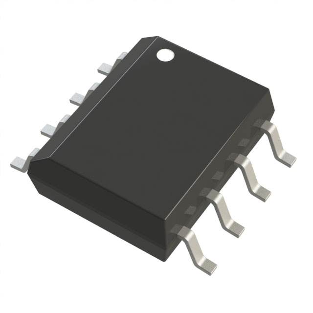
The PBLS2002S,115 is a pre-biased bipolar transistor (BJT) manufactured by NXP USA Inc., combining 1 NPN pre-biased and 1 PNP transistor in a single 8-SO surface mount package. This integrated configuration delivers 1.5W power dissipation with dual-transistor functionality for switching and amplification applications. The part is classified as obsolete, necessitating identification of active substitute components that maintain electrical and mechanical compatibility for ongoing production and maintenance requirements.
Substiute Parts
Key Parameters
| Parameter | Value | Unit |
|---|---|---|
| Transistor Configuration | 1 NPN Pre-Biased, 1 PNP | — |
| Collector Current (Max) - NPN / PNP | 100mA / 3A | A |
| Collector-Emitter Breakdown Voltage (Max) - NPN / PNP | 50V / 20V | V |
| Base Resistor (R1) | 4.7kOhms | Ω |
| Emitter-Base Resistor (R2) | 4.7kOhms | Ω |
| DC Current Gain (hFE Min) @ Ic, Vce | 30 @ 10mA, 5V / 150 @ 2A, 2V | — |
| Vce Saturation (Max) @ Ib, Ic | 150mV @ 500µA, 10mA / 355mV @ 300mA, 3A | V |
| Transition Frequency | 100MHz | MHz |
| Power Dissipation (Max) | 1.5W | W |
| Package Type | 8-SOIC (0.154", 3.90mm Width) | — |
| Mounting Type | Surface Mount | — |
| RoHS Status | ROHS3 Compliant | — |
| MSL Rating | 1 (Unlimited) | — |
Substitute Part Grouping Explanation
Substitution of the PBLS2002S,115 is determined by the following critical parameters:
Electrical Compatibility Criteria:
- Transistor configuration: Dual pre-biased transistor pair (NPN + PNP or PNP + PNP)
- Base and emitter-base resistor values: 4.7kOhms (both R1 and R2)
- Collector current ratings sufficient for application requirements
- Collector-emitter breakdown voltages meeting or exceeding circuit voltage specifications
- DC current gain (hFE) characteristics within acceptable operating ranges
- Transition frequency supporting required switching speeds
Mechanical Compatibility Criteria:
- Surface mount package format
- Pin count and footprint compatibility
- Power dissipation capability
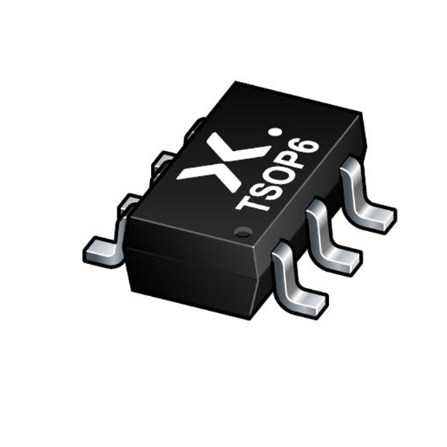
The PBLS2022D,115 qualifies as a substitute based on matching electrical parameters (identical base resistor values, compatible voltage ratings, and equivalent DC current gain specifications) and surface mount configuration. However, the transistor configuration differs (1 PNP Pre-Biased, 1 PNP versus 1 NPN Pre-Biased, 1 PNP), and the package format changes from 8-SO to 6-TSOP, requiring circuit board layout modification.
Parameter Comparison
| Parameter | PBLS2002S,115 | PBLS2022D,115 | Compatibility Notes |
|---|---|---|---|
| Manufacturer | NXP USA Inc. | Nexperia USA Inc. | Related manufacturers |
| Product Status | Obsolete | Active | Substitute is in active production |
| Transistor Type | 1 NPN Pre-Biased, 1 PNP | 1 PNP Pre-Biased, 1 PNP | Configuration differs; circuit topology must be evaluated |
| Collector Current (Max) - Primary / Secondary | 100mA / 3A | 100mA / 1.8A | Secondary current reduced; verify application requirements |
| Collector-Emitter Breakdown (Max) - Primary / Secondary | 50V / 20V | 50V / 20V | Identical voltage ratings |
| Base Resistor (R1) | 4.7kOhms | 4.7kOhms | Identical |
| Emitter-Base Resistor (R2) | 4.7kOhms | 4.7kOhms | Identical |
| DC Current Gain (hFE Min) @ Ic, Vce | 30 @ 10mA, 5V / 150 @ 2A, 2V | 30 @ 10mA, 5V / 200 @ 1A, 2V | Gain characteristics compatible; secondary gain higher at lower current |
| Vce Saturation (Max) @ Ib, Ic | 150mV @ 500µA, 10mA / 355mV @ 300mA, 3A | 150mV @ 500µA, 10mA / 210mV @ 100mA, 1.8A | Primary saturation identical; secondary saturation improved |
| Transition Frequency | 100MHz | 130MHz | Substitute offers higher frequency capability |
| Power Dissipation (Max) | 1.5W | 760mW | Substitute has reduced power rating; verify thermal requirements |
| Package / Case | 8-SOIC (0.154", 3.90mm Width) | SC-74, SOT-457 (6-TSOP) | Different package; PCB layout modification required |
| RoHS Status | ROHS3 Compliant | ROHS3 Compliant | Both compliant |
| MSL Rating | 1 (Unlimited) | 1 (Unlimited) | Identical moisture sensitivity |
Engineering Selection Recommendations
Product Status Consideration: The PBLS2002S,115 is classified as obsolete. The PBLS2022D,115 is an active product from Nexperia USA Inc., ensuring ongoing availability and manufacturing support for new designs and production continuity.
Compliance and Certification: Both components maintain ROHS3 compliance and unlimited moisture sensitivity level (MSL 1), satisfying environmental and handling requirements for industrial and commercial applications.
Substitution Feasibility: Direct substitution requires evaluation of the following factors:
-
Transistor Configuration Change: The PBLS2002S,115 contains 1 NPN pre-biased and 1 PNP transistor, while the PBLS2022D,115 contains 2 PNP pre-biased transistors. Circuit topology and biasing schemes must be reviewed to determine functional equivalence.
-
Secondary Collector Current: The PBLS2022D,115 secondary transistor maximum collector current is 1.8A compared to 3A in the original part. Applications requiring the full 3A capability must verify that 1.8A is sufficient.
-
Power Dissipation: The substitute part is rated for 760mW versus 1.5W. Thermal analysis of the application is required to confirm adequate heat dissipation.
-
Package Footprint: The change from 8-SO to 6-TSOP requires printed circuit board layout modification and re-qualification of assembly processes.
Compliance Verification: Both parts satisfy ROHS3 and REACH requirements. No additional regulatory barriers exist for substitution in compliant applications.
Frequently Asked Questions (FAQ)
Q1: Can the PBLS2022D,115 be used as a direct pin-for-pin replacement for the PBLS2002S,115?
No. The PBLS2022D,115 uses a 6-TSOP package (SC-74, SOT-457) compared to the 8-SOIC package of the original part. Pin count and footprint differ, requiring circuit board redesign. Additionally, the transistor configuration changes from 1 NPN + 1 PNP to 2 PNP, which may affect circuit operation depending on the application topology.
Q2: What are the key electrical parameters that determine substitution compatibility?
Substitution compatibility is determined by: (1) base and emitter-base resistor values (both 4.7kOhms in this case), (2) collector current ratings meeting application requirements, (3) collector-emitter breakdown voltages, (4) DC current gain characteristics, and (5) transition frequency. The PBLS2022D,115 maintains identical resistor values and voltage ratings but differs in transistor configuration and secondary current capability.
Q3: Does the PBLS2022D,115 have sufficient power dissipation for applications using the PBLS2002S,115?
The PBLS2022D,115 is rated for 760mW maximum power dissipation compared to 1.5W for the original part. Applications must be analyzed to determine if the reduced power rating is acceptable. Thermal modeling of the specific circuit application is required.
Q4: Are there any compliance or regulatory differences between these parts?
Both components are ROHS3 compliant and carry unlimited moisture sensitivity level (MSL 1). No regulatory barriers exist for substitution in compliant applications. Both parts are classified as EAR99 for export control purposes.
Q5: What is the impact of the transistor configuration change from NPN+PNP to PNP+PNP?
The configuration change affects circuit biasing and switching behavior. Applications designed around the NPN+PNP combination may require circuit topology modifications to function with the PNP+PNP configuration. Functional equivalence must be verified through circuit analysis and testing.
Q6: Is the higher transition frequency (130MHz vs. 100MHz) of the PBLS2022D,115 a concern?
No. The higher transition frequency of the substitute part (130MHz) is a performance enhancement that does not create compatibility issues. Applications designed for 100MHz operation will function correctly with a component rated for 130MHz.
Q7: What documentation is required before implementing this substitution?
Circuit topology analysis, thermal modeling, package footprint verification, and functional testing are required. The transistor configuration change necessitates detailed evaluation of biasing networks and switching characteristics specific to the application.
Alternative Parts

SJ6012L2TP
Littelfuse Inc.
6 Alternative Parts

JMK107BBJ476MA-RE
Taiyo Yuden
10 Alternative Parts

GMK107BBJ475MA-T
Taiyo Yuden
5 Alternative Parts
SJ6020N2ARP
Littelfuse Inc.
3 Alternative Parts
SJ6025R2ATP
Littelfuse Inc.
4 Alternative Parts

2474-05L
API Delevan Inc.
1 Alternative Parts

4590R-684K
API Delevan Inc.
1 Alternative Parts

CM6560R-334
API Delevan Inc.
1 Alternative Parts

CM6460-104
API Delevan Inc.
1 Alternative Parts

5526-12
API Delevan Inc.
1 Alternative Parts