


Request Quote
(Ships tomorrow)
OPA602BP Equivalent & Substitute Parts
Part Overview
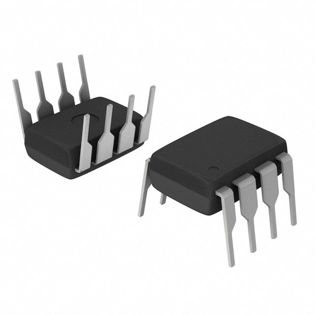
The OPA602BP is a general-purpose operational amplifier manufactured by Texas Instruments, housed in an 8-PDIP through-hole package. This device is classified as obsolete, indicating it is no longer in active production. The OPA602BP operates as a single-circuit amplifier with JFET input technology, delivering a slew rate of 35V/µs and a gain-bandwidth product of 6.5 MHz. Due to its obsolete status, identifying equivalent substitute parts with compatible electrical and mechanical specifications is necessary for design continuity and procurement planning.
Substiute Parts
Key Parameters
| Parameter | Value |
|---|---|
| Manufacturer Part Number | OPA602BP |
| Manufacturer | Texas Instruments |
| Category | Linear, Amplifiers |
| Product Status | Obsolete |
| Amplifier Type | General Purpose |
| Number of Circuits | 1 |
| Slew Rate | 35V/µs |
| Gain Bandwidth Product | 6.5 MHz |
| Current - Input Bias | 1 pA |
| Voltage - Input Offset | 500 µV |
| Current - Supply | 3 mA |
| Current - Output / Channel | 20 mA |
| Voltage - Supply Span (Min) | 10 V |
| Voltage - Supply Span (Max) | 36 V |
| Operating Temperature | -25°C ~ 85°C |
| Mounting Type | Through Hole |
| Package / Case | 8-DIP (0.300", 7.62mm) |
| RoHS Status | ROHS3 Compliant |
| Moisture Sensitivity Level (MSL) | 1 (Unlimited) |
Substitute Part Grouping Explanation
Substitution of the OPA602BP is determined by compatibility across the following critical parameters:
Electrical Compatibility Criteria:
- Single-circuit operational amplifier configuration
- JFET input technology for low input bias current
- Output current capability of 20 mA per channel
- Supply voltage range overlap (minimum 10V to 36V maximum for OPA602BP)
- Operating temperature range that encompasses or exceeds the original specification
Mechanical Compatibility Criteria:
- Package type and pin count (8-pin configuration)
- Mounting technology (through-hole or surface-mount with adapter consideration)
Compliance Criteria:
- RoHS3 compliance
- REACH unaffected status
- Active or obsolete product status
The OPA145IDR is identified as a manufacturer-recommended substitute based on these parameters, though with specific trade-offs in performance characteristics and package form factor.
Parameter Comparison
| Parameter | OPA602BP (Main Part) | OPA145IDR (Substitute) |
|---|---|---|
| Manufacturer | Texas Instruments | Texas Instruments |
| Category | Linear, Amplifiers | Linear, Amplifiers |
| Amplifier Type | General Purpose | J-FET |
| Number of Circuits | 1 | 1 |
| Slew Rate | 35V/µs | 20V/µs |
| Gain Bandwidth Product | 6.5 MHz | 5.5 MHz |
| Current - Input Bias | 1 pA | 2 pA |
| Voltage - Input Offset | 500 µV | 40 µV |
| Current - Supply | 3 mA | 445 µA |
| Current - Output / Channel | 20 mA | 20 mA |
| Voltage - Supply Span (Min) | 10 V | 4.5 V |
| Voltage - Supply Span (Max) | 36 V | 36 V |
| Operating Temperature | -25°C ~ 85°C | -55°C ~ 150°C |
| Mounting Type | Through Hole | Surface Mount |
| Package / Case | 8-DIP (0.300", 7.62mm) | 8-SOIC (0.154", 3.90mm Width) |
| RoHS Status | ROHS3 Compliant | ROHS3 Compliant |
| Moisture Sensitivity Level (MSL) | 1 (Unlimited) | 2 (1 Year) |
Engineering Selection Recommendations
The OPA145IDR is the manufacturer-recommended substitute for the obsolete OPA602BP. Both devices maintain ROHS3 compliance and REACH unaffected status, ensuring regulatory alignment.
Electrical Performance Trade-offs: The OPA145IDR exhibits superior input offset voltage (40 µV versus 500 µV) and significantly reduced supply current (445 µA versus 3 mA), making it advantageous for low-power applications. However, the OPA602BP provides higher slew rate (35V/µs versus 20V/µs) and greater gain-bandwidth product (6.5 MHz versus 5.5 MHz), which may be critical in high-speed signal conditioning circuits.
Supply Voltage Consideration: The OPA145IDR operates at lower minimum supply voltage (4.5 V versus 10 V), expanding application flexibility in battery-powered and low-voltage systems. The maximum supply voltage remains identical at 36 V.
Temperature Range: The OPA145IDR supports an extended operating temperature range (-55°C to 150°C) compared to the OPA602BP (-25°C to 85°C), providing broader environmental compatibility.
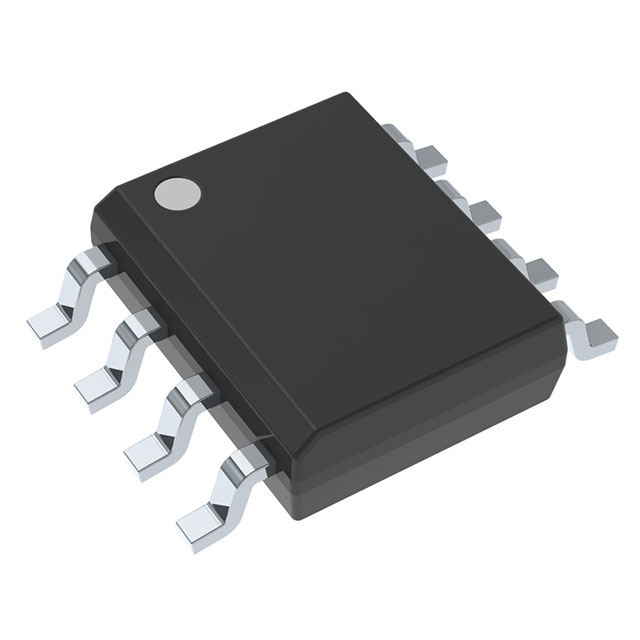
Package and Mounting: The OPA602BP uses through-hole 8-DIP packaging, while the OPA145IDR uses surface-mount 8-SOIC packaging. This represents a fundamental change in assembly methodology and printed circuit board layout requirements. Through-hole to surface-mount conversion requires PCB redesign and different assembly processes.
Product Status: The OPA145IDR maintains active product status with higher inventory availability (5549 pieces versus 1419 pieces), ensuring long-term supply chain stability.
Frequently Asked Questions (FAQ)
Q: Can the OPA145IDR directly replace the OPA602BP in existing designs?
A: Electrical substitution is feasible based on single-circuit JFET amplifier configuration and compatible output current ratings. However, the package change from 8-DIP through-hole to 8-SOIC surface-mount requires PCB redesign and assembly process modification. Pin-to-pin electrical compatibility exists, but physical mounting differs fundamentally.
Q: What are the performance implications of using the OPA145IDR instead of the OPA602BP?
A: The OPA145IDR provides superior input offset voltage (40 µV versus 500 µV) and lower supply current consumption (445 µA versus 3 mA). The OPA602BP maintains advantages in slew rate (35V/µs versus 20V/µs) and gain-bandwidth product (6.5 MHz versus 5.5 MHz). Application-specific requirements determine whether these trade-offs are acceptable.
Q: Is the OPA145IDR suitable for applications requiring the OPA602BP's 10V minimum supply voltage?
A: No. The OPA145IDR operates at a minimum supply voltage of 4.5 V, which is below the OPA602BP's 10 V minimum requirement. Designs dependent on 10 V minimum supply operation require verification that the OPA145IDR's lower threshold does not introduce unintended circuit behavior.
Q: What is the impact of the package change from 8-DIP to 8-SOIC?
A: The package change requires complete PCB redesign, including footprint modification, trace routing adjustments, and assembly process changes from through-hole insertion to surface-mount placement and reflow soldering. This is not a pin-compatible drop-in replacement at the board level.
Q: Are both parts compliant with current regulatory standards?
A: Yes. Both the OPA602BP and OPA145IDR are ROHS3 compliant and REACH unaffected, meeting current regulatory requirements for electronic components.
Q: Why does the OPA145IDR have lower supply current than the OPA602BP?
A: The OPA145IDR is specified at 445 µA supply current versus the OPA602BP's 3 mA. This difference reflects design optimization in the OPA145IDR for low-power operation, making it suitable for battery-powered and energy-constrained applications.
Q: What is the significance of the extended temperature range in the OPA145IDR?
A: The OPA145IDR operates from -55°C to 150°C, compared to the OPA602BP's -25°C to 85°C range. This extended specification accommodates industrial, automotive, and high-temperature applications where the OPA602BP's narrower range is insufficient.
Q: How does the input bias current compare between these devices?
A: Both devices exhibit extremely low input bias current (1 pA for OPA602BP, 2 pA for OPA145IDR), characteristic of JFET input amplifiers. This difference is negligible for most practical applications.
Alternative Parts

SJ6012L2TP
Littelfuse Inc.
6 Alternative Parts

JMK107BBJ476MA-RE
Taiyo Yuden
10 Alternative Parts

GMK107BBJ475MA-T
Taiyo Yuden
5 Alternative Parts
SJ6020N2ARP
Littelfuse Inc.
3 Alternative Parts
SJ6025R2ATP
Littelfuse Inc.
4 Alternative Parts

2474-05L
API Delevan Inc.
1 Alternative Parts

4590R-684K
API Delevan Inc.
1 Alternative Parts

CM6560R-334
API Delevan Inc.
1 Alternative Parts

CM6460-104
API Delevan Inc.
1 Alternative Parts

5526-12
API Delevan Inc.
1 Alternative Parts