


Request Quote
(Ships tomorrow)
NVMFS5C612NLAFT3G Equivalent & Substitute Parts
Part Overview
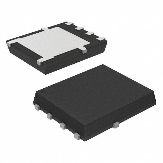
The NVMFS5C612NLAFT3G is an N-Channel 60V MOSFET manufactured by onsemi, designed for surface mount applications in the 5-DFN (5x6) package. This device delivers 38A continuous drain current at 25°C (Ta) and 250A at case temperature (Tc), with a maximum on-resistance of 1.36 mOhm at 50A and 10V gate-source voltage. The part is qualified to AEC-Q101 automotive standards and operates across a temperature range of -55°C to 175°C.
The NVMFS5C612NLAFT3G carries a product status of "Not For New Designs," indicating that onsemi has transitioned this part to end-of-life status. Organizations requiring this MOSFET for new applications or ongoing production must identify functionally equivalent alternatives that maintain electrical and mechanical compatibility while offering active product status.
Substiute Parts
Key Parameters
| Parameter | Value | Unit |
|---|---|---|
| Drain to Source Voltage (Vdss) | 60 | V |
| Continuous Drain Current @ 25°C (Ta) | 38 | A |
| Continuous Drain Current @ Case Temp (Tc) | 250 | A |
| On-Resistance (Rds On Max) @ 50A, 10V | 1.36 | mOhm |
| Gate-Source Threshold Voltage (Vgs(th)) @ 250µA | 2 | V |
| Gate Charge (Qg) @ 10V | 91 | nC |
| Input Capacitance (Ciss) @ 25V | 6660 | pF |
| Maximum Gate-Source Voltage | ±20 | V |
| Power Dissipation (Ta) | 3.8 | W |
| Power Dissipation (Tc) | 167 | W |
| Operating Temperature Range | -55 to 175 | °C |
| Package Type | 8-PowerTDFN, 5 Leads | 5-DFN (5x6) |
| Mounting Type | Surface Mount | |
| Automotive Grade | AEC-Q101 | |
| RoHS Status | ROHS3 Compliant |
Substitute Part Grouping Explanation
Substitution of the NVMFS5C612NLAFT3G is determined by electrical and mechanical parameter equivalence across the following criteria:
Electrical Parameters (Must Match):
- Drain to Source Voltage (Vdss): 60V
- Continuous Drain Current: 38A (Ta), 250A (Tc)
- On-Resistance (Rds On): 1.36 mOhm @ 50A, 10V
- Gate-Source Threshold Voltage: 2V @ 250µA
- Gate Charge: 91 nC @ 10V
- Input Capacitance: 6660 pF @ 25V
- Maximum Gate-Source Voltage: ±20V
- Power Dissipation: 3.8W (Ta), 167W (Tc)
- Operating Temperature Range: -55°C to 175°C
Mechanical Parameters (Must Match):
- Package Type: 8-PowerTDFN, 5 Leads (5-DFN 5x6)
- Mounting Type: Surface Mount
- Supplier Device Package: 5-DFN (5x6) (8-SOFL)
Compliance & Qualification (Must Match):
- Automotive Grade: AEC-Q101
- RoHS Status: ROHS3 Compliant
- Moisture Sensitivity Level: 1 (Unlimited)
The identified substitute parts maintain identical electrical performance and package specifications. Differences in product status and mounting surface treatment do not affect functional equivalence in circuit applications.
Parameter Comparison
| Parameter | NVMFS5C612NLAFT3G | NVMFS5C612NLAFT1G | NVMFS5C612NLWFAFT1G |
|---|---|---|---|
| Manufacturer | onsemi | onsemi | onsemi |
| FET Type | N-Channel | N-Channel | N-Channel |
| Technology | MOSFET (Metal Oxide) | MOSFET (Metal Oxide) | MOSFET (Metal Oxide) |
| Drain to Source Voltage (Vdss) | 60V | 60V | 60V |
| Continuous Drain Current (Ta) | 38A | 38A | 38A |
| Continuous Drain Current (Tc) | 250A | 250A | 250A |
| On-Resistance (Rds On Max) @ 50A, 10V | 1.36 mOhm | 1.36 mOhm | 1.36 mOhm |
| Gate-Source Threshold Voltage @ 250µA | 2V | 2V | 2V |
| Gate Charge @ 10V | 91 nC | 91 nC | 91 nC |
| Input Capacitance @ 25V | 6660 pF | 6660 pF | 6660 pF |
| Maximum Gate-Source Voltage | ±20V | ±20V | ±20V |
| Power Dissipation (Ta) | 3.8W | 3.8W | 3.8W |
| Power Dissipation (Tc) | 167W | 167W | 167W |
| Operating Temperature Range | -55°C to 175°C | -55°C to 175°C | -55°C to 175°C |
| Package Type | 8-PowerTDFN, 5 Leads | 8-PowerTDFN, 5 Leads | 8-PowerTDFN, 5 Leads |
| Supplier Device Package | 5-DFN (5x6) (8-SOFL) | 5-DFN (5x6) (8-SOFL) | 5-DFN (5x6) (8-SOFL) |
| Mounting Type | Surface Mount | Surface Mount | Surface Mount, Wettable Flank |
| Automotive Grade | AEC-Q101 | AEC-Q101 | AEC-Q101 |
| RoHS Status | ROHS3 Compliant | ROHS3 Compliant | ROHS3 Compliant |
| Moisture Sensitivity Level | 1 (Unlimited) | 1 (Unlimited) | 1 (Unlimited) |
| Product Status | Not For New Designs | Active | Active |
Engineering Selection Recommendations
NVMFS5C612NLAFT1G is the primary substitute for the NVMFS5C612NLAFT3G. This part maintains complete electrical and mechanical equivalence while offering active product status from onsemi. The transition from "Not For New Designs" to "Active" status ensures long-term availability and supply chain continuity. Both parts are AEC-Q101 qualified and ROHS3 compliant, meeting automotive and environmental regulatory requirements. The NVMFS5C612NLAFT1G is suitable for direct replacement in existing designs and for new product development.
NVMFS5C612NLWFAFT1G provides an alternative with identical electrical specifications and active product status. This variant incorporates a wettable flank surface treatment on the package, which enhances solder joint inspection capability during manufacturing. The wettable flank feature does not alter electrical performance or thermal characteristics. Selection of this variant depends on manufacturing process requirements and quality assurance protocols. Organizations employing automated optical inspection (AOI) systems may benefit from the improved solder joint visibility provided by the wettable flank design.
Both substitute parts share the same base product number (NVMFS5) and are manufactured by onsemi using identical MOSFET technology. Electrical performance, thermal management, and reliability characteristics remain unchanged across all three part numbers.
Frequently Asked Questions (FAQ)
Q: Can NVMFS5C612NLAFT1G be used as a direct replacement for NVMFS5C612NLAFT3G?
A: Yes. The NVMFS5C612NLAFT1G is electrically and mechanically equivalent to the NVMFS5C612NLAFT3G. All electrical parameters, including Vdss, drain current, on-resistance, gate charge, and operating temperature range, are identical. Both parts use the same 8-PowerTDFN package with 5 leads. The primary difference is product status: NVMFS5C612NLAFT1G is active, while NVMFS5C612NLAFT3G is not recommended for new designs.
Q: What is the difference between NVMFS5C612NLAFT1G and NVMFS5C612NLWFAFT1G?
A: Both parts are electrically identical with matching Vdss, drain current, on-resistance, and thermal specifications. The difference is in the mounting surface treatment. NVMFS5C612NLWFAFT1G includes a wettable flank feature, which extends the solder coating to the side edges of the package. This feature improves visibility of solder joints during automated optical inspection. Electrical performance and thermal characteristics are unchanged.
Q: Are these parts suitable for automotive applications?
A: Yes. All three parts carry AEC-Q101 automotive qualification and are ROHS3 compliant. They meet automotive industry standards for reliability and environmental compliance. The operating temperature range of -55°C to 175°C supports automotive thermal requirements.
Q: What is the moisture sensitivity level for these MOSFETs?
A: All three parts have a Moisture Sensitivity Level (MSL) of 1, which indicates unlimited shelf life without moisture control requirements. These parts do not require special dry-pack storage or baking procedures prior to assembly.
Q: Can I use NVMFS5C612NLWFAFT1G in applications where NVMFS5C612NLAFT1G was specified?
A: Yes. The wettable flank variant is electrically and thermally equivalent. The only difference is the manufacturing surface treatment, which does not affect circuit performance. Selection between the two depends on manufacturing process requirements and inspection capabilities.
Q: What is the package type for these MOSFETs?
A: All three parts use the 8-PowerTDFN package with 5 leads, designated as 5-DFN (5x6) (8-SOFL). This is a surface mount package suitable for automated assembly processes.
Q: Are there any differences in gate charge or input capacitance between these parts?
A: No. All three parts have identical gate charge (91 nC @ 10V) and input capacitance (6660 pF @ 25V). These parameters determine switching speed and drive circuit requirements, and they are unchanged across all three part numbers.
Q: What is the maximum on-resistance for these MOSFETs?
A: The maximum on-resistance is 1.36 mOhm, measured at 50A drain current and 10V gate-source voltage. This specification is identical across all three parts and determines power dissipation in switching applications.
Alternative Parts

SJ6012L2TP
Littelfuse Inc.
6 Alternative Parts

JMK107BBJ476MA-RE
Taiyo Yuden
10 Alternative Parts

GMK107BBJ475MA-T
Taiyo Yuden
5 Alternative Parts
SJ6020N2ARP
Littelfuse Inc.
3 Alternative Parts
SJ6025R2ATP
Littelfuse Inc.
4 Alternative Parts

2474-05L
API Delevan Inc.
1 Alternative Parts

4590R-684K
API Delevan Inc.
1 Alternative Parts

CM6560R-334
API Delevan Inc.
1 Alternative Parts

CM6460-104
API Delevan Inc.
1 Alternative Parts

5526-12
API Delevan Inc.
1 Alternative Parts