


Request Quote
(Ships tomorrow)
NTTS2P02R2 P-Channel MOSFET Equivalent & Substitute Parts
Part Overview
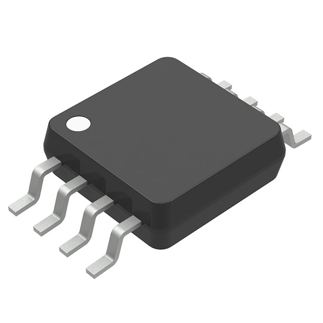
The NTTS2P02R2 is a P-Channel MOSFET manufactured by onsemi, rated for 20V drain-to-source voltage with 2.4A continuous drain current at 25°C. The device is housed in an 8-MSOP surface mount package and is designed for low-power switching applications requiring compact form factors.
This part carries an Obsolete product status. Identifying equivalent and substitute components is necessary to maintain design continuity, ensure supply chain reliability, and support ongoing production requirements for applications currently utilizing this device.
Substiute Parts
Key Parameters
| Parameter | Value | Unit |
|---|---|---|
| Manufacturer Part Number | NTTS2P02R2 | — |
| Manufacturer | onsemi | — |
| FET Type | P-Channel | — |
| Drain-to-Source Voltage (Vdss) | 20 | V |
| Continuous Drain Current (Id) @ 25°C | 2.4 | A |
| On-Resistance (Rds On) @ 2.4A, 4.5V | 90 | mOhm |
| Gate Threshold Voltage (Vgs(th)) @ 250µA | 1.4 | V (Max) |
| Gate Charge (Qg) @ 4.5V | 18 | nC (Max) |
| Maximum Gate Voltage (Vgs) | ±8 | V |
| Input Capacitance (Ciss) @ 16V | 550 | pF (Max) |
| Power Dissipation (Max) | 780 | mW |
| Operating Temperature Range | -55 to 150 | °C (TJ) |
| Package Type | 8-MSOP | — |
| Mounting Type | Surface Mount | — |
| Product Status | Obsolete | — |
| RoHS Status | RoHS non-compliant | — |
Substitute Part Grouping Explanation
Substitution of the NTTS2P02R2 is determined by strict adherence to the following electrical and mechanical parameters:
Critical Matching Parameters:
- FET Type: P-Channel topology
- Drain-to-Source Voltage (Vdss): 20V minimum rating
- Package Type: 8-MSOP surface mount configuration
- Operating Temperature Range: -55°C to 150°C (TJ)
- On-Resistance (Rds On): 90mOhm @ 2.4A, 4.5V
Allowable Substitution Criteria: Substitute parts must maintain identical or superior electrical performance within the specified parameter envelope. The ZXM64P02XTA from Diodes Incorporated satisfies substitution requirements through matching Vdss rating, identical package geometry, overlapping temperature range, and equivalent on-resistance specification. The substitute part demonstrates higher continuous drain current capability (3.5A versus 2.4A) and increased power dissipation rating (1.1W versus 780mW), providing design margin without introducing incompatibility.
Parameter Comparison
| Parameter | NTTS2P02R2 (onsemi) | ZXM64P02XTA (Diodes Inc.) | Unit |
|---|---|---|---|
| FET Type | P-Channel | P-Channel | — |
| Drain-to-Source Voltage (Vdss) | 20 | 20 | V |
| Continuous Drain Current (Id) @ 25°C | 2.4 | 3.5 | A |
| On-Resistance (Rds On) @ 2.4A, 4.5V | 90 | 90 | mOhm |
| Gate Threshold Voltage (Vgs(th)) @ 250µA | 1.4 (Max) | 0.7 (Min) | V |
| Gate Charge (Qg) @ 4.5V | 18 | 6.9 | nC (Max) |
| Maximum Gate Voltage (Vgs) | ±8 | ±12 | V |
| Input Capacitance (Ciss) @ Vds | 550 @ 16V | 900 @ 15V | pF (Max) |
| Power Dissipation (Max) | 780 | 1100 | mW |
| Operating Temperature Range | -55 to 150 | -55 to 150 | °C (TJ) |
| Package Type | 8-MSOP | 8-MSOP | — |
| Mounting Type | Surface Mount | Surface Mount | — |
| Product Status | Obsolete | Active | — |
| RoHS Status | RoHS non-compliant | ROHS3 Compliant | — |
Engineering Selection Recommendations
Primary Substitute: ZXM64P02XTA (Diodes Incorporated)
The ZXM64P02XTA is the qualified substitute for the obsolete NTTS2P02R2. This selection is based on the following engineering factors:
Product Status Alignment: The ZXM64P02XTA carries Active product status, ensuring long-term availability and continued manufacturer support. The NTTS2P02R2 Obsolete designation creates supply chain risk and limits access to new inventory.
Electrical Compatibility: Both devices share identical Vdss (20V) and Rds On (90mOhm @ 2.4A, 4.5V) specifications. The ZXM64P02XTA provides higher continuous drain current (3.5A) and power dissipation capability (1.1W), delivering design margin for existing applications without requiring circuit modification.
Package and Mechanical Compatibility: Both parts utilize the 8-MSOP surface mount package with identical 0.118" (3.00mm) width, enabling direct PCB footprint compatibility and automated assembly without layout revision.
Compliance and Certification: The ZXM64P02XTA achieves ROHS3 compliance, addressing regulatory requirements for new designs and manufacturing environments. Both devices maintain REACH Unaffected and EAR99 ECCN classifications.
Temperature Performance: Operating temperature ranges are identical (-55°C to 150°C TJ), ensuring thermal performance equivalence across the full application envelope.
Frequently Asked Questions (FAQ)
Q: Can the ZXM64P02XTA directly replace the NTTS2P02R2 without circuit modification?
A: Yes. Both devices share identical Vdss (20V), Rds On (90mOhm @ 2.4A, 4.5V), and operating temperature range (-55°C to 150°C). The 8-MSOP package geometry is identical, enabling direct PCB footprint compatibility. The ZXM64P02XTA's higher current rating (3.5A versus 2.4A) and power dissipation (1.1W versus 780mW) provide design margin without requiring circuit changes.
Q: What are the key electrical differences between these two P-Channel MOSFETs?
A: The primary differences are continuous drain current (ZXM64P02XTA: 3.5A versus NTTS2P02R2: 2.4A), power dissipation (ZXM64P02XTA: 1.1W versus NTTS2P02R2: 780mW), gate charge (ZXM64P02XTA: 6.9nC versus NTTS2P02R2: 18nC), and maximum gate voltage (ZXM64P02XTA: ±12V versus NTTS2P02R2: ±8V). On-resistance and Vdss ratings are identical.
Q: Are there packaging considerations when substituting these parts?
A: No. Both devices use the 8-MSOP surface mount package with identical 0.118" (3.00mm) width. PCB footprints, solder pad layouts, and automated assembly processes require no modification.
Q: Why is the NTTS2P02R2 marked as Obsolete?
A: Obsolete status indicates the manufacturer (onsemi) has discontinued production and support for this device. The ZXM64P02XTA Active status ensures continued availability, technical support, and manufacturing consistency.
Q: Does the ZXM64P02XTA meet current regulatory requirements?
A: Yes. The ZXM64P02XTA is ROHS3 compliant, addressing current environmental and regulatory standards. The NTTS2P02R2 is RoHS non-compliant, which may restrict use in new designs or manufacturing environments subject to RoHS regulations.
Q: What is the significance of the lower gate charge in the ZXM64P02XTA?
A: The ZXM64P02XTA gate charge (6.9nC @ 4.5V) is lower than the NTTS2P02R2 (18nC @ 4.5V). Lower gate charge reduces switching losses and driver power requirements, providing improved efficiency in switching applications without affecting DC operating characteristics.
Q: Can the ZXM64P02XTA be used in applications requiring the full ±8V gate voltage range of the NTTS2P02R2?
A: Yes. The ZXM64P02XTA supports ±12V maximum gate voltage, which encompasses the ±8V range of the NTTS2P02R2. Applications utilizing ±8V gate drive are fully compatible.
Alternative Parts

SJ6012L2TP
Littelfuse Inc.
6 Alternative Parts

JMK107BBJ476MA-RE
Taiyo Yuden
10 Alternative Parts

GMK107BBJ475MA-T
Taiyo Yuden
5 Alternative Parts
SJ6020N2ARP
Littelfuse Inc.
3 Alternative Parts
SJ6025R2ATP
Littelfuse Inc.
4 Alternative Parts

2474-05L
API Delevan Inc.
1 Alternative Parts

4590R-684K
API Delevan Inc.
1 Alternative Parts

CM6560R-334
API Delevan Inc.
1 Alternative Parts

CM6460-104
API Delevan Inc.
1 Alternative Parts

5526-12
API Delevan Inc.
1 Alternative Parts