


Request Quote
(Ships tomorrow)
NTMFS4926NET1G Equivalent & Substitute Parts
Part Overview
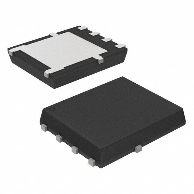
The NTMFS4926NET1G is an N-Channel MOSFET manufactured by onsemi, rated for 30V drain-to-source voltage with continuous drain current of 9A at Ta and 44A at Tc. The device is housed in a 5-DFN (5x6) surface mount package and is designed for general-purpose switching applications requiring moderate power dissipation handling.
This part carries an Obsolete product status. Identifying equivalent and substitute components is necessary to maintain design continuity, ensure supply chain reliability, and support ongoing production requirements for applications currently utilizing this device.
Substiute Parts
Key Parameters
| Parameter | Value | Unit |
|---|---|---|
| Drain-to-Source Voltage (Vdss) | 30 | V |
| Continuous Drain Current @ 25°C (Ta) | 9 | A |
| Continuous Drain Current @ 25°C (Tc) | 44 | A |
| RDS(on) Max @ Id, Vgs | 7 mOhm @ 30A, 10V | mOhm |
| Gate Threshold Voltage (Vgs(th)) Max | 2.2 | V @ 250µA |
| Gate Charge (Qg) Max @ Vgs | 17.3 | nC @ 10V |
| Input Capacitance (Ciss) Max @ Vds | 1004 | pF @ 15V |
| Power Dissipation Max (Ta) | 920 | mW |
| Power Dissipation Max (Tc) | 21.6 | W |
| Operating Temperature Range | -55 to 150 | °C (TJ) |
| Package Type | 5-DFN (5x6) | Surface Mount |
| Moisture Sensitivity Level | 1 | Unlimited |
Substitute Part Grouping Explanation
Substitution of the NTMFS4926NET1G is determined by electrical and mechanical compatibility across the following critical parameters:
Electrical Compatibility Criteria:
- Drain-to-Source Voltage (Vdss) must equal or exceed 30V
- Continuous drain current ratings (both Ta and Tc conditions) must meet or exceed the original specification
- On-resistance (RDS(on)) characteristics must support equivalent switching performance
- Gate threshold voltage and gate charge must be compatible with existing drive circuitry
- Input capacitance must not introduce unacceptable switching delays
- Operating temperature range must encompass -55°C to 150°C
Mechanical Compatibility Criteria:
- Surface mount package type must be compatible with existing PCB layouts
- Lead configuration and footprint must accommodate the application
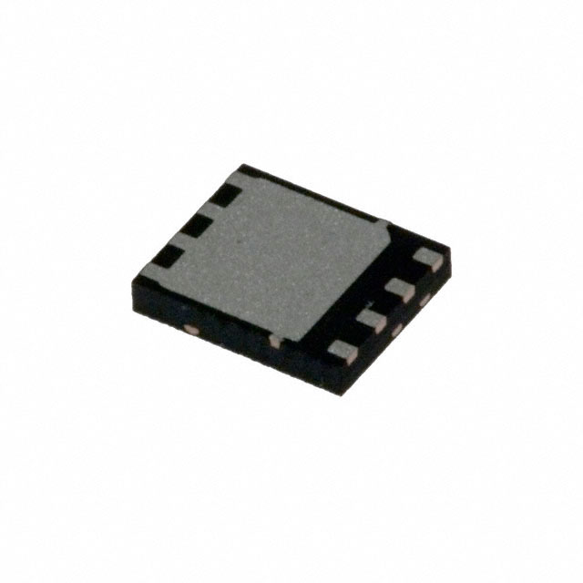
The CSD17308Q3 from Texas Instruments satisfies these substitution criteria through equivalent voltage ratings, superior current handling capabilities, and compatible surface mount packaging, while maintaining the same operating temperature range and moisture sensitivity classification.
Parameter Comparison
| Parameter | NTMFS4926NET1G (onsemi) | CSD17308Q3 (Texas Instruments) | Unit |
|---|---|---|---|
| Drain-to-Source Voltage (Vdss) | 30 | 30 | V |
| Continuous Drain Current @ Ta | 9 | 14 | A |
| Continuous Drain Current @ Tc | 44 | 44 | A |
| RDS(on) Max @ Vgs | 7 mOhm @ 10V | 10.3 mOhm @ 8V | mOhm |
| Gate Threshold Voltage (Vgs(th)) Max | 2.2 | 1.8 | V @ 250µA |
| Gate Charge (Qg) Max | 17.3 | 5.1 | nC |
| Input Capacitance (Ciss) Max @ 15V | 1004 | 700 | pF |
| Power Dissipation Max (Ta) | 920 | 2700 | mW |
| Operating Temperature Range | -55 to 150 | -55 to 150 | °C (TJ) |
| Mounting Type | Surface Mount | Surface Mount | |
| Moisture Sensitivity Level | 1 | 1 | Unlimited |
| REACH Status | REACH Unaffected | REACH Unaffected | |
| ECCN Classification | EAR99 | EAR99 |
Engineering Selection Recommendations
Product Status Consideration: The NTMFS4926NET1G carries an Obsolete designation, making the CSD17308Q3 the appropriate substitute for ongoing production and design continuity. The CSD17308Q3 maintains Active product status with Texas Instruments, ensuring long-term availability and supply chain stability.
Compliance and Certification Alignment: Both devices share identical REACH Unaffected status and EAR99 ECCN classification, confirming regulatory compatibility. Both devices maintain Moisture Sensitivity Level 1 (Unlimited), indicating no special handling requirements during storage or assembly.
Electrical Performance: The CSD17308Q3 provides superior continuous drain current at Ta (14A versus 9A), matching the Tc rating of 44A. The substitute device demonstrates lower gate charge (5.1 nC versus 17.3 nC) and reduced input capacitance (700 pF versus 1004 pF), resulting in faster switching characteristics and reduced driver loading. The on-resistance specification of the substitute (10.3 mOhm @ 8V) remains within acceptable operating parameters for equivalent thermal performance.
Package and Thermal Considerations: The CSD17308Q3 utilizes an 8-VSON-CLIP (3.3x3.3) package, which differs from the original 5-DFN (5x6) footprint. PCB layout modification is required to accommodate this package change. The substitute device offers improved thermal performance through its package design, supporting higher power dissipation at Ta (2.7W versus 920mW).
Frequently Asked Questions (FAQ)
Q: Can the CSD17308Q3 directly replace the NTMFS4926NET1G without circuit modifications?
A: Electrical substitution is valid based on voltage rating, current capability, and operating temperature range. However, the package footprint differs (8-VSON-CLIP versus 5-DFN), requiring PCB layout redesign. Gate drive voltage compatibility must be verified; the CSD17308Q3 operates with a maximum gate voltage of ±10V/-8V compared to the original ±20V specification.
Q: What are the key advantages of the CSD17308Q3 as a substitute?
A: The substitute device offers higher continuous drain current at Ta (14A versus 9A), significantly lower gate charge (5.1 nC versus 17.3 nC) enabling faster switching, reduced input capacitance (700 pF versus 1004 pF) for lower driver loading, and Active product status ensuring long-term availability. The device maintains identical voltage rating and Tc current capability.
Q: Are there thermal performance differences between these devices?
A: The CSD17308Q3 supports higher power dissipation at Ta (2.7W versus 920mW) due to its package design. Both devices maintain identical Tc power dissipation capability (21.6W). Thermal performance improvement in the substitute device results from superior package thermal characteristics rather than die-level changes.
Q: What PCB design considerations apply when switching to the CSD17308Q3?
A: The 8-VSON-CLIP (3.3x3.3) package requires footprint redesign compared to the 5-DFN (5x6) original. The smaller package footprint may reduce PCB area requirements. Thermal via placement and copper area allocation should be optimized for the new package geometry to achieve equivalent thermal performance.
Q: Are there any gate drive circuit modifications required?
A: The CSD17308Q3 specifies a maximum gate voltage of +10V/-8V, compared to the original ±20V rating. Existing gate drive circuits operating within ±10V/-8V parameters require no modification. Circuits utilizing the full ±20V range must be redesigned to limit gate voltage to the substitute device specification.
Q: How do the switching characteristics compare between these devices?
A: The CSD17308Q3 exhibits significantly lower gate charge (5.1 nC versus 17.3 nC) and reduced input capacitance (700 pF versus 1004 pF), resulting in faster switching transitions and reduced switching losses. These characteristics benefit high-frequency switching applications and reduce gate driver power consumption.
Q: What is the supply chain status difference between these parts?
A: The NTMFS4926NET1G is classified as Obsolete, indicating discontinued production and limited availability. The CSD17308Q3 maintains Active status with Texas Instruments, ensuring continued manufacturing, documented availability, and long-term design support.
Alternative Parts

SJ6012L2TP
Littelfuse Inc.
6 Alternative Parts

JMK107BBJ476MA-RE
Taiyo Yuden
10 Alternative Parts

GMK107BBJ475MA-T
Taiyo Yuden
5 Alternative Parts
SJ6020N2ARP
Littelfuse Inc.
3 Alternative Parts
SJ6025R2ATP
Littelfuse Inc.
4 Alternative Parts

2474-05L
API Delevan Inc.
1 Alternative Parts

4590R-684K
API Delevan Inc.
1 Alternative Parts

CM6560R-334
API Delevan Inc.
1 Alternative Parts

CM6460-104
API Delevan Inc.
1 Alternative Parts

5526-12
API Delevan Inc.
1 Alternative Parts