


Request Quote
(Ships tomorrow)
NTMFS4845NT1G Equivalent & Substitute Parts
Part Overview
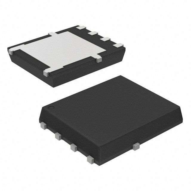
The NTMFS4845NT1G is an N-Channel MOSFET manufactured by onsemi, rated for 30V drain-to-source voltage with continuous drain current of 13.7A at Ta and 115A at Tc. The device is housed in a 5-DFN (5x6) surface mount package and is designed for general-purpose switching applications requiring low on-resistance performance.
This part is classified as Obsolete, necessitating identification of equivalent alternatives for ongoing production and design requirements. Substitute parts must maintain electrical compatibility across voltage ratings, current handling, thermal characteristics, and package form factors while meeting current manufacturing and compliance standards.
Substiute Parts
Key Parameters
| Parameter | Value | Unit |
|---|---|---|
| Drain-to-Source Voltage (Vdss) | 30 | V |
| Continuous Drain Current @ Ta | 13.7 | A |
| Continuous Drain Current @ Tc | 115 | A |
| On-Resistance (Rds On Max) @ 30A, 10V | 2.9 | mOhm |
| Gate Threshold Voltage (Vgs(th)) @ 250µA | 2.5 | V |
| Gate Charge (Qg) @ 11.5V | 62 | nC |
| Input Capacitance (Ciss) @ 12V | 3720 | pF |
| Power Dissipation @ Ta | 890 | mW |
| Power Dissipation @ Tc | 62.5 | W |
| Operating Temperature Range | -55 to 150 | °C |
| Package Type | 5-DFN (5x6) | Surface Mount |
| RoHS Status | ROHS3 Compliant |
Substitute Part Grouping Explanation
Substitution of the NTMFS4845NT1G is determined by the following critical electrical and mechanical parameters:
Voltage Rating Compatibility: The substitute part must maintain a Vdss rating of 30V to ensure safe operation within the same voltage domain.
Current Handling Capacity: The substitute must support continuous drain current specifications that meet or exceed the original part's 13.7A (Ta) and 115A (Tc) ratings to ensure thermal and electrical performance equivalence.
On-Resistance Characteristics: The Rds On specification directly impacts power dissipation and thermal performance. Substitute parts must demonstrate comparable or superior on-resistance values to maintain efficiency.
Gate Charge and Input Capacitance: These parameters affect switching speed and gate drive requirements. Substitutes must remain within acceptable ranges to prevent circuit redesign.
Thermal Performance: Power dissipation ratings at both ambient (Ta) and case (Tc) temperatures must support the application's thermal budget.
Package Compatibility: While the original part uses a 5-DFN package, substitute parts may employ alternative surface mount packages provided they are compatible with the PCB layout and thermal management strategy.
Compliance and Product Status: Substitute parts must maintain RoHS3 compliance and preferably be in active production status to ensure long-term availability.
Parameter Comparison
| Parameter | NTMFS4845NT1G (onsemi) | PSMN3R0-30YL,115 (Nexperia) | Unit |
|---|---|---|---|
| Manufacturer | onsemi | Nexperia USA Inc. | |
| FET Type | N-Channel | N-Channel | |
| Technology | MOSFET (Metal Oxide) | MOSFET (Metal Oxide) | |
| Drain-to-Source Voltage (Vdss) | 30 | 30 | V |
| Continuous Drain Current @ Tc | 115 | 100 | A |
| On-Resistance (Rds On Max) | 2.9 @ 30A, 10V | 3.0 @ 15A, 10V | mOhm |
| Gate Threshold Voltage (Vgs(th)) | 2.5 @ 250µA | 2.15 @ 1mA | V |
| Gate Charge (Qg) | 62 @ 11.5V | 45.8 @ 10V | nC |
| Input Capacitance (Ciss) | 3720 @ 12V | 2822 @ 12V | pF |
| Power Dissipation @ Tc | 62.5 | 81 | W |
| Operating Temperature Range | -55 to 150 | -55 to 175 | °C |
| Mounting Type | Surface Mount | Surface Mount | |
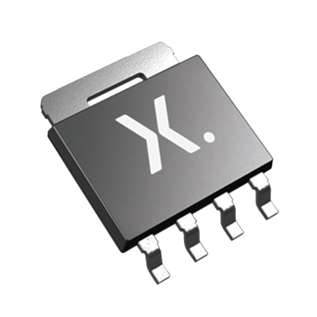
| Package Type | 5-DFN (5x6) | LFPAK56 | |
| Product Status | Obsolete | Not For New Designs | |
| RoHS Status | ROHS3 Compliant | ROHS3 Compliant | |
| MSL Rating | 1 (Unlimited) | 1 (Unlimited) |
Engineering Selection Recommendations
PSMN3R0-30YL,115 (Nexperia USA Inc.) serves as an electrical equivalent to the NTMFS4845NT1G based on the following criteria:
Voltage Domain Alignment: Both parts operate at 30V Vdss, ensuring direct compatibility in voltage-constrained applications.
Current Capacity: The PSMN3R0-30YL,115 provides 100A continuous drain current at Tc, which is slightly lower than the original part's 115A rating. This difference is acceptable for applications where the design margin accommodates the 13% reduction in thermal current capacity.
On-Resistance Performance: The PSMN3R0-30YL,115 exhibits 3.0 mOhm on-resistance compared to the original 2.9 mOhm. This marginal increase (3.4%) results in proportionally higher power dissipation but remains within acceptable engineering tolerances for most switching applications.
Gate Drive Characteristics: The substitute part demonstrates lower gate charge (45.8 nC vs. 62 nC) and reduced input capacitance (2822 pF vs. 3720 pF), resulting in faster switching transitions and reduced gate drive power requirements.
Thermal Operating Range: The PSMN3R0-30YL,115 extends the maximum junction temperature to 175°C compared to the original 150°C, providing enhanced thermal margin in high-temperature environments.
Compliance Status: Both parts maintain ROHS3 compliance and unlimited moisture sensitivity level (MSL 1), ensuring compatibility with standard manufacturing and storage protocols.
Product Availability: While the PSMN3R0-30YL,115 is classified as "Not For New Designs," it remains in active inventory (42,862 units available) and provides a viable transition path for existing production requirements.
Package Consideration: The substitute employs an LFPAK56 package instead of the original 5-DFN form factor. PCB layout modifications are required to accommodate the different package geometry and thermal pad configuration.
Frequently Asked Questions (FAQ)
Q: Can the PSMN3R0-30YL,115 be used as a direct pin-for-pin replacement for the NTMFS4845NT1G?
A: No. While both parts are N-Channel MOSFETs with identical 30V ratings, they employ different package types (5-DFN vs. LFPAK56). PCB layout redesign is required to accommodate the different package footprint and thermal pad dimensions. Pin configuration must be verified against the respective datasheets before implementation.
Q: What is the impact of the 15A reduction in continuous drain current (115A to 100A)?
A: The PSMN3R0-30YL,115 provides 100A continuous drain current at Tc, representing an 13% reduction from the original specification. For applications operating below 100A, this difference is not significant. Applications requiring the full 115A capacity must evaluate alternative substitutes or implement thermal management enhancements to maintain safe operating margins.
Q: How does the lower gate charge of the substitute part affect circuit design?
A: The PSMN3R0-30YL,115 exhibits 45.8 nC gate charge compared to the original 62 nC, a 26% reduction. This results in faster switching transitions and reduced gate drive power consumption. Existing gate drive circuits designed for the original part will operate with improved performance margins and reduced power dissipation.
Q: Are there thermal management differences between the two packages?
A: The 5-DFN and LFPAK56 packages have different thermal pad geometries and thermal resistance characteristics. The LFPAK56 package is designed for higher power dissipation applications. Thermal analysis specific to the PCB layout and thermal management strategy is required to ensure equivalent thermal performance.
Q: What compliance certifications are maintained with the substitute part?
A: The PSMN3R0-30YL,115 maintains ROHS3 compliance, REACH unaffected status, and MSL 1 (unlimited) moisture sensitivity rating, identical to the original part. Both parts are classified under ECCN EAR99 and HTSUS 8541.29.0095.
Q: Why is the PSMN3R0-30YL,115 classified as "Not For New Designs"?
A: This classification indicates that while the part remains available in inventory, the manufacturer is not actively promoting it for new design implementations. However, it remains a valid substitute for existing production requirements and legacy system support.
Q: What is the significance of the extended operating temperature range (-55°C to 175°C vs. -55°C to 150°C)?
A: The substitute part's extended upper temperature limit of 175°C provides an additional 25°C thermal margin compared to the original 150°C specification. This allows operation in higher ambient temperature environments without exceeding maximum junction temperature limits.
Alternative Parts

SJ6012L2TP
Littelfuse Inc.
6 Alternative Parts

JMK107BBJ476MA-RE
Taiyo Yuden
10 Alternative Parts

GMK107BBJ475MA-T
Taiyo Yuden
5 Alternative Parts
SJ6020N2ARP
Littelfuse Inc.
3 Alternative Parts
SJ6025R2ATP
Littelfuse Inc.
4 Alternative Parts

2474-05L
API Delevan Inc.
1 Alternative Parts

4590R-684K
API Delevan Inc.
1 Alternative Parts

CM6560R-334
API Delevan Inc.
1 Alternative Parts

CM6460-104
API Delevan Inc.
1 Alternative Parts

5526-12
API Delevan Inc.
1 Alternative Parts