


Request Quote
(Ships tomorrow)
NCP500SQL50T1G Equivalent & Substitute Parts
Part Overview
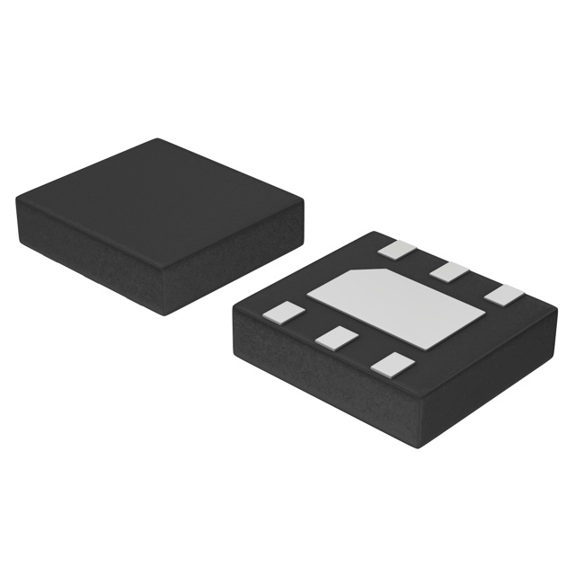
The NCP500SQL50T1G is a linear voltage regulator IC from onsemi designed for positive fixed 5V output at 150mA in a 6-DFN (2x2.2) surface mount package. This component is classified as obsolete, making identification of suitable substitute parts essential for ongoing design support and production continuity. The regulator features integrated over-current and over-temperature protection with enable control functionality.
Substiute Parts
Key Parameters
| Parameter | Value |
|---|---|
| Manufacturer Part Number | NCP500SQL50T1G |
| Manufacturer | onsemi |
| Category | Power Management (PMIC) |
| Output Voltage (Fixed) | 5V |
| Output Current | 150mA |
| Input Voltage (Max) | 6V |
| Voltage Dropout (Max) | 0.18V @ 150mA |
| Package / Case | 6-VDFN Exposed Pad |
| Operating Temperature | -40°C ~ 85°C (TA) |
| Product Status | Obsolete |
| RoHS Status | ROHS3 Compliant |
Substitute Part Grouping Explanation
Substitution of the NCP500SQL50T1G is determined by the following critical parameters:
Fixed Output Voltage: 5V output is the primary functional requirement. Substitute parts must maintain this exact output voltage.
Output Current Capability: The NCP500SQL50T1G delivers 150mA. Substitute parts with equal or greater current capacity are acceptable for direct replacement.
Package Compatibility: The 6-VDFN Exposed Pad package defines the physical footprint. Substitute parts in equivalent DFN packages with matching pin configuration are suitable.
Input Voltage Range: Maximum input voltage of 6V establishes the input specification. Substitute parts must accommodate this voltage range.
Protection Features: Over-current and over-temperature protection are standard requirements. Substitute parts must include these protection mechanisms.
Compliance & Status: RoHS3 compliance and active product status are preferred for long-term availability and regulatory alignment.
Parameter Comparison
| Parameter | NCP500SQL50T1G | NCP718AMT500TBG |
|---|---|---|
| Manufacturer | onsemi | onsemi |
| Output Voltage (Fixed) | 5V | 5V |
| Output Current | 150mA | 300mA |
| Input Voltage (Max) | 6V | 24V |
| Voltage Dropout (Max) | 0.18V @ 150mA | 0.38V @ 300mA |
| Quiescent Current (Iq) | 1 µA | 8 µA |
| PSRR | 62dB (1kHz) | 60dB (1kHz) |
| Package / Case | 6-VDFN Exposed Pad | 6-WDFN Exposed Pad |
| Operating Temperature | -40°C ~ 85°C (TA) | -40°C ~ 125°C (TJ) |
| Product Status | Obsolete | Active |
| RoHS Status | ROHS3 Compliant | ROHS3 Compliant |
Engineering Selection Recommendations
The NCP718AMT500TBG is a direct functional substitute for the NCP500SQL50T1G based on the following criteria:
Output Voltage Match: Both parts deliver fixed 5V output, meeting the primary functional requirement.
Current Capacity: The NCP718AMT500TBG provides 300mA output current, exceeding the 150mA requirement of the original part. This provides design margin and supports higher load conditions without modification.
Active Product Status: The NCP718AMT500TBG is classified as active, ensuring long-term availability and manufacturing support. This addresses the obsolescence of the original NCP500SQL50T1G.
Compliance Alignment: Both parts maintain ROHS3 compliance and identical REACH and ECCN classifications, ensuring regulatory continuity.
Package Consideration: The NCP718AMT500TBG uses a 6-WDFN package versus the 6-VDFN of the original part. Both are 6-pin DFN packages with exposed pads in similar physical dimensions (2x2 mm footprint). PCB layout verification is required to confirm mechanical compatibility.
Extended Operating Range: The NCP718AMT500TBG supports -40°C to 125°C junction temperature, providing broader thermal operating margin compared to the -40°C to 85°C ambient specification of the original part.
Frequently Asked Questions (FAQ)
Q: Can the NCP718AMT500TBG directly replace the NCP500SQL50T1G without circuit modifications?
A: The NCP718AMT500TBG is functionally compatible for 5V fixed output applications. Both parts feature enable control and integrated protection. However, verify PCB footprint compatibility between the 6-VDFN and 6-WDFN packages before implementation. Pin configuration must be confirmed against the respective datasheets.
Q: What is the significance of the higher output current rating on the NCP718AMT500TBG?
A: The NCP718AMT500TBG delivers 300mA versus 150mA on the original part. This increased capacity allows the substitute to support higher load currents without thermal stress, providing design flexibility for applications requiring current headroom.
Q: Does the extended input voltage range of the NCP718AMT500TBG affect compatibility?
A: The NCP718AMT500TBG accepts input voltages up to 24V, compared to 6V maximum on the NCP500SQL50T1G. This broader input range does not create incompatibility; it simply provides additional design flexibility. Applications limited to 6V input will operate identically on both parts.
Q: Are there package-related considerations for PCB redesign?
A: The original NCP500SQL50T1G uses a 6-VDFN package; the substitute NCP718AMT500TBG uses a 6-WDFN package. Both are surface mount DFN packages with similar footprints. Verify pin-to-pin compatibility and PCB layout spacing before production implementation.
Q: Why is product status important for this substitution?
A: The NCP500SQL50T1G is obsolete, limiting future availability and manufacturing support. The NCP718AMT500TBG is active, ensuring consistent supply and ongoing technical support from onsemi for production and design applications.
Alternative Parts

SJ6012L2TP
Littelfuse Inc.
6 Alternative Parts

JMK107BBJ476MA-RE
Taiyo Yuden
10 Alternative Parts

GMK107BBJ475MA-T
Taiyo Yuden
5 Alternative Parts
SJ6020N2ARP
Littelfuse Inc.
3 Alternative Parts
SJ6025R2ATP
Littelfuse Inc.
4 Alternative Parts

2474-05L
API Delevan Inc.
1 Alternative Parts

4590R-684K
API Delevan Inc.
1 Alternative Parts

CM6560R-334
API Delevan Inc.
1 Alternative Parts

CM6460-104
API Delevan Inc.
1 Alternative Parts

5526-12
API Delevan Inc.
1 Alternative Parts