


Request Quote
(Ships tomorrow)
NC7SV08P5X Equivalent & Substitute Parts
Part Overview
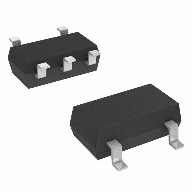
The NC7SV08P5X is a single-channel AND gate logic IC manufactured by onsemi, housed in a 5-TSSOP (SC-70-5) surface mount package. This component operates across a supply voltage range of 0.9V to 3.6V and is designed for low-power logic applications requiring minimal quiescent current. The part maintains Active product status with full RoHS3 compliance and unlimited moisture sensitivity rating. Equivalent and substitute parts are identified based on matching logic function, package compatibility, and electrical parameter alignment within acceptable operational ranges.
Substiute Parts
Key Parameters
| Parameter | Value |
|---|---|
| Logic Type | AND Gate |
| Number of Circuits | 1 |
| Number of Inputs | 2 |
| Voltage - Supply | 0.9V ~ 3.6V |
| Current - Quiescent (Max) | 900 nA |
| Current - Output High, Low | 24mA, 24mA |
| Input Logic Level - Low | 0.7V ~ 0.8V |
| Input Logic Level - High | 1.6V ~ 2V |
| Max Propagation Delay @ V, Max CL | 2.3ns @ 3V, 30pF |
| Operating Temperature | -40°C ~ 85°C |
| Package / Case | 5-TSSOP, SC-70-5, SOT-353 |
| Mounting Type | Surface Mount |
| RoHS Status | ROHS3 Compliant |
| Moisture Sensitivity Level (MSL) | 1 (Unlimited) |
Substitute Part Grouping Explanation
Substitute parts for the NC7SV08P5X are qualified based on the following criteria:
Functional Equivalence: All substitute parts must implement a single-channel, 2-input AND gate logic function.
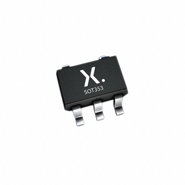
Package Compatibility: Substitute parts must use the 5-TSSOP (SC-70-5, SOT-353) surface mount package to ensure direct PCB footprint compatibility.
Electrical Parameter Alignment: Supply voltage range, input logic levels, and output drive capability must support the operational requirements of the original design. Propagation delay and quiescent current characteristics must fall within acceptable ranges for the application.
Compliance & Status: All substitute parts must maintain Active product status and RoHS3 compliance to ensure long-term availability and regulatory conformance.
The identified substitutes—74AUP1G08GW,125 (Nexperia) and SN74AUC1G08DCKR (Texas Instruments)—meet these criteria while offering alternative sourcing options from established logic IC manufacturers.
Parameter Comparison
| Parameter | NC7SV08P5X (onsemi) | 74AUP1G08GW,125 (Nexperia) | SN74AUC1G08DCKR (Texas Instruments) |
|---|---|---|---|
| Logic Type | AND Gate | AND Gate | AND Gate |
| Number of Circuits | 1 | 1 | 1 |
| Number of Inputs | 2 | 2 | 2 |
| Voltage - Supply | 0.9V ~ 3.6V | 0.8V ~ 3.6V | 0.8V ~ 2.7V |
| Current - Quiescent (Max) | 900 nA | 500 nA | 10 µA |
| Current - Output High, Low | 24mA, 24mA | 4mA, 4mA | 9mA, 9mA |
| Input Logic Level - Low | 0.7V ~ 0.8V | 0.7V ~ 0.9V | 0.7V |
| Input Logic Level - High | 1.6V ~ 2V | 1.6V ~ 2V | 1.7V |
| Max Propagation Delay @ V, Max CL | 2.3ns @ 3V, 30pF | 6.2ns @ 3.3V, 30pF | 2ns @ 2.5V, 30pF |
| Operating Temperature | -40°C ~ 85°C | -40°C ~ 125°C | -40°C ~ 85°C |
| Package / Case | 5-TSSOP, SC-70-5, SOT-353 | 5-TSSOP, SC-70-5, SOT-353 | 5-TSSOP, SC-70-5, SOT-353 |
| Mounting Type | Surface Mount | Surface Mount | Surface Mount |
| RoHS Status | ROHS3 Compliant | ROHS3 Compliant | ROHS3 Compliant |
| Moisture Sensitivity Level (MSL) | 1 (Unlimited) | 1 (Unlimited) | 1 (Unlimited) |
Engineering Selection Recommendations
All three parts maintain Active product status and full RoHS3 compliance, ensuring regulatory conformance and long-term supply viability. The NC7SV08P5X remains the primary reference part with established inventory availability of 23,400 units.
The 74AUP1G08GW,125 (Nexperia) offers superior quiescent current performance at 500 nA and extended operating temperature range to 125°C, making it suitable for ultra-low-power and high-temperature applications. However, output drive capability is reduced to 4mA compared to the primary part's 24mA, and propagation delay increases to 6.2ns.
The SN74AUC1G08DCKR (Texas Instruments) provides the fastest propagation delay at 2ns and moderate output drive at 9mA. Its supply voltage range is limited to 0.8V to 2.7V, which excludes operation at the upper 3.6V specification of the primary part. Quiescent current is higher at 10 µA.
Selection between substitutes depends on application-specific requirements for power consumption, temperature range, output drive capability, and supply voltage constraints.
Frequently Asked Questions (FAQ)
Q: Can the 74AUP1G08GW,125 directly replace the NC7SV08P5X in all applications?
A: The 74AUP1G08GW,125 shares identical package and logic function but has reduced output drive current (4mA vs. 24mA) and slower propagation delay (6.2ns vs. 2.3ns). Substitution is valid only if the application does not require the higher output drive capability or faster switching speed of the original part.
Q: What is the impact of the SN74AUC1G08DCKR's 2.7V maximum supply voltage?
A: The SN74AUC1G08DCKR cannot operate at the NC7SV08P5X's maximum specified supply voltage of 3.6V. This part is suitable only for applications with supply voltages not exceeding 2.7V. Designs operating at 3.3V or higher must use the NC7SV08P5X or 74AUP1G08GW,125.
Q: Are all three parts pin-compatible?
A: Yes. All three parts use the 5-TSSOP (SC-70-5, SOT-353) package with identical pin
Alternative Parts

SJ6012L2TP
Littelfuse Inc.
6 Alternative Parts

JMK107BBJ476MA-RE
Taiyo Yuden
10 Alternative Parts

GMK107BBJ475MA-T
Taiyo Yuden
5 Alternative Parts
SJ6020N2ARP
Littelfuse Inc.
3 Alternative Parts
SJ6025R2ATP
Littelfuse Inc.
4 Alternative Parts

2474-05L
API Delevan Inc.
1 Alternative Parts

4590R-684K
API Delevan Inc.
1 Alternative Parts

CM6560R-334
API Delevan Inc.
1 Alternative Parts

CM6460-104
API Delevan Inc.
1 Alternative Parts

5526-12
API Delevan Inc.
1 Alternative Parts