


Request Quote
(Ships tomorrow)
MPC9229FN Equivalent & Substitute Parts
Part Overview
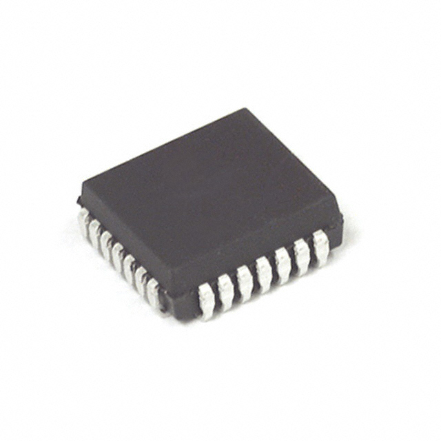
The MPC9229FN is a Clock/Frequency Synthesizer and Clock Generator IC manufactured by NXP USA Inc., designed for 400MHz operation in a 28-LCC (J-Lead) surface mount package. This device features a Phase-Locked Loop (PLL) with bypass capability, crystal input, and LVPECL output configuration. The MPC9229FN is classified as obsolete, making identification of functionally equivalent substitute components necessary for ongoing system support and new design implementations.
Substiute Parts
Key Parameters
| Parameter | Value |
|---|---|
| Manufacturer Part Number | MPC9229FN |
| Manufacturer | NXP USA Inc. |
| Category | Clock/Timing |
| Type | Clock/Frequency Synthesizer, Clock Generator |
| Frequency - Max | 400 MHz |
| Input Type | Crystal |
| Output Type | LVPECL |
| Ratio - Input:Output | 1:1 |
| PLL Configuration | Yes with Bypass |
| Voltage - Supply | 3.135V ~ 3.465V |
| Operating Temperature | 0°C ~ 70°C |
| Package / Case | 28-LCC (J-Lead) |
| Mounting Type | Surface Mount |
| Product Status | Obsolete |
| RoHS Status | RoHS non-compliant |
| MSL Rating | 1 (Unlimited) |
Substitute Part Grouping Explanation
Substitution of the MPC9229FN is determined by the following critical parameters:
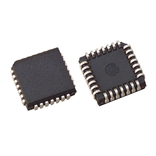
- Package Compatibility: Both main and substitute parts must use 28-LCC (J-Lead) surface mount packaging with identical footprint dimensions (11.51x11.51mm)
- Output Signal Type: LVPECL output is required for signal integrity and impedance matching in clock distribution networks
- Frequency Range: Substitute parts must support minimum 400 MHz operation to maintain system timing specifications
- Supply Voltage: Operating voltage range must encompass or exceed the 3.135V ~ 3.465V requirement
- Functional Classification: Clock/timing ICs with fanout buffer or synthesis capabilities that maintain signal distribution integrity
The CDCVF111FN qualifies as a substitute based on these parameters, despite functional differences in input:output ratio and maximum frequency capability.
Parameter Comparison
| Parameter | MPC9229FN (Main) | CDCVF111FN (Substitute) |
|---|---|---|
| Manufacturer | NXP USA Inc. | Texas Instruments |
| Category | Clock/Timing | Clock/Timing |
| Package / Case | 28-LCC (J-Lead) | 28-LCC (J-Lead) |
| Supplier Device Package | 28-PLCC (11.51x11.51) | 28-PLCC (11.51x11.51) |
| Mounting Type | Surface Mount | Surface Mount |
| Output Type | LVPECL | LVPECL |
| Frequency - Max | 400 MHz | 650 MHz |
| Voltage - Supply | 3.135V ~ 3.465V | 3V ~ 3.6V |
| Operating Temperature | 0°C ~ 70°C | -40°C ~ 85°C |
| MSL Rating | 1 (Unlimited) | 1 (Unlimited) |
| RoHS Status | RoHS non-compliant | ROHS3 Compliant |
| REACH Status | REACH Unaffected | REACH Unaffected |
| ECCN | EAR99 | EAR99 |
| HTSUS Code | 8542.39.0001 | 8542.39.0001 |
Engineering Selection Recommendations
Product Status Consideration: The MPC9229FN is obsolete, while the CDCVF111FN is active. For new designs or long-term system support, the CDCVF111FN provides continued availability and manufacturing support from Texas Instruments.
Compliance Status: The CDCVF111FN meets ROHS3 compliance requirements, whereas the MPC9229FN is RoHS non-compliant. Systems requiring RoHS compliance must transition to the CDCVF111FN.
Electrical Compatibility: The CDCVF111FN supply voltage range (3V ~ 3.6V) encompasses the MPC9229FN requirement (3.135V ~ 3.465V), ensuring compatible power delivery. The extended maximum frequency (650 MHz vs. 400 MHz) and expanded operating temperature range (-40°C ~ 85°C vs. 0°C ~ 70°C) provide additional operational margin.
Package and Footprint: Both devices use identical 28-LCC (J-Lead) packaging with 11.51x11.51mm footprint dimensions, enabling direct PCB layout compatibility without redesign.
Frequently Asked Questions (FAQ)
Q: Can the CDCVF111FN directly replace the MPC9229FN in existing designs?
A: Physical and electrical compatibility exists due to identical package geometry, LVPECL output signaling, and overlapping supply voltage specifications. However, functional differences in input:output ratio (1:9 vs. 1:1) and circuit topology require circuit-level evaluation to confirm suitability for specific applications.
Q: What is the significance of the 1:9 input:output ratio in the CDCVF111FN?
A: The CDCVF111FN functions as a fanout buffer, distributing a single input clock signal to nine output channels. The MPC9229FN operates as a 1:1 synthesizer. Application requirements determine whether multi-output distribution or single-output synthesis is needed.
Q: Are there supply voltage compatibility concerns?
A: The CDCVF111FN supply range (3V ~ 3.6V) fully encompasses the MPC9229FN specification (3.135V ~ 3.465V). Standard 3.3V supply rails used in most applications support both devices without modification.
Q: Does the 28-LCC package ensure PCB compatibility?
A: Yes. Both devices use identical 28-LCC (J-Lead) packaging with matching 11.51x11.51mm footprint dimensions. PCB layouts designed for the MPC9229FN accommodate the CDCVF111FN without trace or via repositioning.
Q: What compliance advantages does the CDCVF111FN offer?
A: The CDCVF111FN is ROHS3 compliant and active in production, whereas the MPC9229FN is obsolete and RoHS non-compliant. Systems subject to environmental or regulatory compliance requirements must use the CDCVF111FN.
Q: How do operating temperature ranges compare?
A: The CDCVF111FN supports -40°C ~ 85°C, exceeding the MPC9229FN range of 0°C ~ 70°C. Applications requiring extended temperature operation benefit from the CDCVF111FN's broader specification.
Alternative Parts

SJ6012L2TP
Littelfuse Inc.
6 Alternative Parts

JMK107BBJ476MA-RE
Taiyo Yuden
10 Alternative Parts

GMK107BBJ475MA-T
Taiyo Yuden
5 Alternative Parts
SJ6020N2ARP
Littelfuse Inc.
3 Alternative Parts
SJ6025R2ATP
Littelfuse Inc.
4 Alternative Parts

2474-05L
API Delevan Inc.
1 Alternative Parts

4590R-684K
API Delevan Inc.
1 Alternative Parts

CM6560R-334
API Delevan Inc.
1 Alternative Parts

CM6460-104
API Delevan Inc.
1 Alternative Parts

5526-12
API Delevan Inc.
1 Alternative Parts