


Request Quote
(Ships tomorrow)
MPC905DR2 Equivalent & Substitute Parts
Part Overview
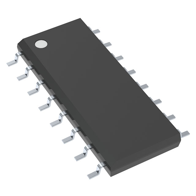
The MPC905DR2 is a Clock Fanout Buffer (Distribution) IC manufactured by NXP USA Inc., designed for 1:6 clock distribution at frequencies up to 100 MHz. This component features TTL/Crystal input compatibility with LVCMOS output, operating across a 3V to 3.6V supply range in a 16-SOIC surface mount package.
The MPC905DR2 is classified as obsolete. Locating equivalent or substitute components becomes necessary when original stock is depleted or when design flexibility permits the use of active alternatives that maintain functional compatibility within the application's electrical and mechanical constraints.
Substiute Parts
Key Parameters
| Parameter | Value |
|---|---|
| Manufacturer | NXP USA Inc. |
| Part Number | MPC905DR2 |
| Category | Clock/Timing |
| Type | Fanout Buffer (Distribution) |
| Package / Case | 16-SOIC (0.154", 3.90mm Width) |
| Mounting Type | Surface Mount |
| Number of Circuits | 1 |
| Ratio - Input:Output | 1:6 |
| Input Type | TTL, Crystal |
| Output Type | LVCMOS |
| Frequency - Max | 100 MHz |
| Voltage - Supply | 3V ~ 3.6V |
| Operating Temperature | 0°C ~ 70°C |
| Product Status | Obsolete |
| RoHS Status | RoHS non-compliant |
| Moisture Sensitivity Level (MSL) | 1 (Unlimited) |
Substitute Part Grouping Explanation
Substitution of the MPC905DR2 is evaluated based on the following critical parameters that define functional and mechanical compatibility:
Package Compatibility: Both the main part and substitute must use the 16-SOIC (0.154", 3.90mm Width) surface mount package to ensure PCB layout compatibility without redesign.
Supply Voltage Range: The substitute must operate within or encompass the 3V to 3.6V supply range specified for the MPC905DR2.
Frequency Capability: The substitute's maximum frequency rating must meet or exceed the 100 MHz operational requirement.
Input/Output Signal Levels: The substitute must accept compatible input signal types and provide compatible output signal levels for the application circuit.
Mounting Type: Surface mount technology must be maintained for assembly process compatibility.
The CDCVF25081DR from Texas Instruments satisfies these core substitution criteria. While it functions as a PLL Clock Driver rather than a simple fanout buffer, and features a 2:8 ratio with enhanced frequency capability (200 MHz), it maintains the identical 16-SOIC package footprint, operates within the specified 3V to 3.6V supply range, and provides compatible signal level translation suitable for clock distribution applications.
Parameter Comparison
| Parameter | MPC905DR2 (NXP) | CDCVF25081DR (Texas Instruments) |
|---|---|---|
| Manufacturer | NXP USA Inc. | Texas Instruments |
| Category | Clock/Timing | Clock/Timing |
| Type | Fanout Buffer (Distribution) | PLL Clock Driver |
| Package / Case | 16-SOIC (0.154", 3.90mm Width) | 16-SOIC (0.154", 3.90mm Width) |
| Mounting Type | Surface Mount | Surface Mount |
| Number of Circuits | 1 | 1 |
| Ratio - Input:Output | 1:6 | 2:8 |
| Voltage - Supply | 3V ~ 3.6V | 3V ~ 3.6V |
| Frequency - Max | 100 MHz | 200 MHz |
| Operating Temperature | 0°C ~ 70°C | -40°C ~ 85°C |
| Product Status | Obsolete | Active |
| RoHS Status | RoHS non-compliant | ROHS3 Compliant |
| Moisture Sensitivity Level (MSL) | 1 (Unlimited) | 1 (Unlimited) |
Engineering Selection Recommendations
Product Status Consideration: The MPC905DR2 is obsolete, whereas the CDCVF25081DR maintains active status with ongoing manufacturer support and availability. Selection of the CDCVF25081DR ensures access to current inventory and technical documentation.
Compliance Status: The CDCVF25081DR is ROHS3 compliant, meeting current environmental and regulatory requirements. The MPC905DR2 is RoHS non-compliant, which may present constraints in applications subject to RoHS directives or customer specifications requiring compliant components.
Package and Thermal Characteristics: Both components share identical 16-SOIC packaging, eliminating PCB redesign requirements. The CDCVF25081DR operates across an extended temperature range (-40°C to 85°C) compared to the MPC905DR2 (0°C to 70°C), providing broader environmental suitability.
Functional Capability: The CDCVF25081DR's 200 MHz maximum frequency and PLL architecture with bypass capability exceed the MPC905DR2's 100 MHz fanout buffer specification, ensuring performance headroom for clock distribution applications.
Frequently Asked Questions (FAQ)
Q: Can the CDCVF25081DR directly replace the MPC905DR2 without PCB modifications?
A: Yes. Both components use the identical 16-SOIC (0.154", 3.90mm Width) surface mount package, enabling direct footprint compatibility without PCB layout changes.
Q: What are the key differences between these two clock distribution components?
A: The MPC905DR2 is a simple 1:6 fanout buffer with 100 MHz maximum frequency. The CDCVF25081DR is a PLL Clock Driver with 2:8 output ratio and 200 MHz capability. Both operate within the 3V to 3.6V supply range and use identical packaging.
Q: Does the higher frequency rating of the CDCVF25081DR affect compatibility?
A: No. The CDCVF25081DR's 200 MHz capability exceeds the MPC905DR2's 100 MHz requirement, providing performance margin. Applications operating at or below 100 MHz remain fully compatible.
Q: Are there supply voltage considerations when substituting?
A: Both components operate within the 3V to 3.6V supply range. No supply voltage modifications are required for substitution.
Q: What is the significance of the CDCVF25081DR's PLL with Bypass feature?
A: The PLL with bypass capability provides design flexibility, allowing operation in either PLL-enabled or bypass modes depending on application requirements. This does not prevent use as a direct substitute in fanout buffer applications.
Q: How do the input signal type specifications compare?
A: The MPC905DR2 accepts TTL and Crystal inputs with LVCMOS outputs. The CDCVF25081DR accepts LVTTL input with LVTTL output. LVTTL is compatible with TTL-level signals, maintaining signal integrity in clock distribution circuits.
Q: Does the extended operating temperature range of the CDCVF25081DR present any concerns?
A: No. The CDCVF25081DR's extended range (-40°C to 85°C) encompasses the MPC905DR2's range (0°C to 70°C), providing equal or superior performance across all specified operating conditions.
Q: What is the impact of RoHS compliance differences?
A: The CDCVF25081DR is ROHS3 compliant, meeting current environmental standards. If the application or customer specification requires RoHS compliance, the CDCVF25081DR is the appropriate selection.
Alternative Parts

SJ6012L2TP
Littelfuse Inc.
6 Alternative Parts

JMK107BBJ476MA-RE
Taiyo Yuden
10 Alternative Parts

GMK107BBJ475MA-T
Taiyo Yuden
5 Alternative Parts
SJ6020N2ARP
Littelfuse Inc.
3 Alternative Parts
SJ6025R2ATP
Littelfuse Inc.
4 Alternative Parts

2474-05L
API Delevan Inc.
1 Alternative Parts

4590R-684K
API Delevan Inc.
1 Alternative Parts

CM6560R-334
API Delevan Inc.
1 Alternative Parts

CM6460-104
API Delevan Inc.
1 Alternative Parts

5526-12
API Delevan Inc.
1 Alternative Parts