


Request Quote
(Ships tomorrow)
MPC555LFMVR40 Equivalent & Substitute Parts
Part Overview
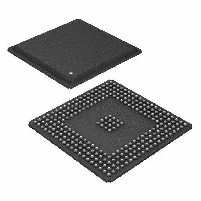
The MPC555LFMVR40 is a PowerPC MPC5xx 32-bit single-core microcontroller featuring 448KB FLASH memory, designed for embedded applications requiring CANbus, SPI, UART/USART, and EBI/EMI connectivity. The device operates at 40MHz with a 272-PBGA package and supports a supply voltage range of 2.7V to 5.5V. This part is currently in Last Time Buy status, making identification of equivalent alternatives essential for ongoing design support and production continuity.
Substiute Parts
Key Parameters
| Parameter | Value |
|---|---|
| Manufacturer Part Number | MPC555LFMVR40 |
| Manufacturer | NXP USA Inc. |
| Core Processor | PowerPC |
| Core Size | 32-Bit Single-Core |
| Speed | 40MHz |
| Program Memory Size | 448KB (448K x 8) FLASH |
| RAM Size | 26K x 8 |
| Voltage Supply (Vcc/Vdd) | 2.7V ~ 5.5V |
| Number of I/O | 101 |
| Connectivity | CANbus, EBI/EMI, SCI, SPI, UART/USART |
| Data Converters | A/D 32x10b |
| Operating Temperature | -40°C ~ 125°C (TA) |
| Package | 272-PBGA (27x27) |
| Product Status | Last Time Buy |
| RoHS Status | ROHS3 Compliant |
Substitute Part Grouping Explanation
The TMS5701114CZWTQQ1 is identified as a manufacturer-recommended substitute for the MPC555LFMVR40. Substitution eligibility is determined by the following critical parameters:
Core Compatibility Criteria:
- Both devices support 32-bit processing architecture
- Both provide CANbus connectivity for automotive and industrial applications
- Both include SPI, UART/USART, and EBI/EMI interfaces
- Both operate across the -40°C to 125°C temperature range
- Both comply with ROHS3 and REACH standards
- Both feature external oscillator configuration
- Both are rated for industrial/automotive embedded applications
Functional Equivalence Parameters:
- Program memory capacity (448KB vs. 1MB) — substitute provides expanded memory
- I/O count (101 pins on both devices) — pin-compatible functionality
- Supply voltage range (2.7V–5.5V vs. 1.14V–3.6V) — substitute supports lower voltage operation
- Data converter specifications (A/D 32x10b vs. A/D 24x12b) — substitute provides enhanced resolution
Package Consideration:
- MPC555LFMVR40: 272-PBGA (27x27)
- TMS5701114CZWTQQ1: 337-NFBGA (16x16)
- Different physical packages require PCB redesign
Parameter Comparison
| Parameter | MPC555LFMVR40 | TMS5701114CZWTQQ1 |
|---|---|---|
| Manufacturer | NXP USA Inc. | Texas Instruments |
| Core Processor | PowerPC | ARM® Cortex®-R4F |
| Core Size | 32-Bit Single-Core | 16/32-Bit |
| Speed | 40MHz | 180MHz |
| Program Memory Size | 448KB FLASH | 1MB FLASH |
| RAM Size | 26K x 8 | 128K x 8 |
| EEPROM Size | — | 64K x 8 |
| Voltage Supply (Vcc/Vdd) | 2.7V ~ 5.5V | 1.14V ~ 3.6V |
| Number of I/O | 101 | 101 |
| Connectivity | CANbus, EBI/EMI, SCI, SPI, UART/USART | CANbus, EBI/EMI, I2C, LINbus, MibSPI, SCI, SPI, UART/USART |
| Peripherals | POR, PWM, WDT | DMA, POR, PWM, WDT |
| Data Converters | A/D 32x10b | A/D 24x12b |
| Operating Temperature | -40°C ~ 125°C (TA) | -40°C ~ 125°C (TA) |
| Package | 272-PBGA (27x27) | 337-NFBGA (16x16) |
| Product Status | Last Time Buy | Active |
| Grade | — | Automotive |
| Qualification | — | AEC-Q100 |
| RoHS Status | ROHS3 Compliant | ROHS3 Compliant |
| MSL Rating | 3 (168 Hours) | 3 (168 Hours) |
Engineering Selection Recommendations
Product Status Consideration: The MPC555LFMVR40 is designated Last Time Buy, indicating NXP has ceased production and will no longer accept new orders beyond a specified cutoff date. The TMS5701114CZWTQQ1 maintains Active product status with Texas Instruments, ensuring long-term availability and ongoing technical support.
Compliance and Certification: Both devices meet ROHS3 and REACH compliance requirements. The TMS5701114CZWTQQ1 carries AEC-Q100 automotive qualification, providing additional assurance for safety-critical applications. Both devices maintain identical MSL ratings (3, 168 Hours).
Functional Advantages of Substitute: The TMS5701114CZWTQQ1 provides increased processing speed (180MHz vs. 40MHz), expanded program memory (1MB vs. 448KB), and additional RAM (128K x 8 vs. 26K x 8). The substitute includes integrated EEPROM (64K x 8) and DMA peripheral support. Extended connectivity options include I2C and LINbus interfaces not present in the original device.
Design Integration Requirements: Substitution requires PCB redesign due to different package geometries (272-PBGA 27x27 vs. 337-NFBGA 16x16). Firmware migration from PowerPC to ARM Cortex-R4F architecture is necessary. Supply voltage range differs (2.7V–5.5V vs. 1.14V–3.6V), requiring power supply circuit evaluation.
Frequently Asked Questions (FAQ)
Q: Can the TMS5701114CZWTQQ1 directly replace the MPC555LFMVR40 without PCB modification?
A: No. The devices use different package types and pin counts. The MPC555LFMVR40 uses 272-PBGA (27x27) while the TMS5701114CZWTQQ1 uses 337-NFBGA (16x16). PCB redesign is required for physical integration.
Q: What are the key electrical differences between these devices?
A: The supply voltage range differs: MPC555LFMVR40 operates at 2.7V–5.5V while TMS5701114CZWTQQ1 operates at 1.14V–3.6V. Processing speed increases from 40MHz to 180MHz. Program memory expands from 448KB to 1MB, and RAM increases from 26K x 8 to 128K x 8.
Q: Are both devices suitable for automotive applications?
A: The MPC555LFMVR40 supports automotive connectivity (CANbus) and operates across the required temperature range. The TMS5701114CZWTQQ1 carries explicit automotive qualification (AEC-Q100) and Automotive grade designation, providing additional certification for safety-critical automotive systems.
Q: What firmware changes are necessary for substitution?
A: The MPC555LFMVR40 uses PowerPC architecture while the TMS5701114CZWTQQ1 uses ARM Cortex-R4F architecture. Complete firmware recompilation and functional validation are required. Peripheral register maps and interrupt handling differ between architectures.
Q: Do both devices support the same communication protocols?
A: Both support CANbus, SPI, UART/USART, and EBI/EMI interfaces. The TMS5701114CZWTQQ1 adds I2C, LINbus, and MibSPI support. Existing CANbus and SPI implementations are compatible, but additional protocol support requires driver development.
Q: What is the impact of increased processing speed on power consumption?
A: The TMS5701114CZWTQQ1 operates at 180MHz compared to 40MHz on the MPC555LFMVR40. Higher clock frequency typically increases power consumption. Detailed power analysis requires evaluation of specific application workload and clock gating strategies.
Q: Are the I/O pin counts equivalent?
A: Both devices provide 101 I/O pins. However, physical pin locations and package geometry differ, requiring complete PCB layout redesign and signal routing validation.
Alternative Parts

SJ6012L2TP
Littelfuse Inc.
6 Alternative Parts

JMK107BBJ476MA-RE
Taiyo Yuden
10 Alternative Parts

GMK107BBJ475MA-T
Taiyo Yuden
5 Alternative Parts
SJ6020N2ARP
Littelfuse Inc.
3 Alternative Parts
SJ6025R2ATP
Littelfuse Inc.
4 Alternative Parts

2474-05L
API Delevan Inc.
1 Alternative Parts

4590R-684K
API Delevan Inc.
1 Alternative Parts

CM6560R-334
API Delevan Inc.
1 Alternative Parts

CM6460-104
API Delevan Inc.
1 Alternative Parts

5526-12
API Delevan Inc.
1 Alternative Parts