


Request Quote
(Ships tomorrow)
MAX988ESA Equivalent & Substitute Parts
Part Overview
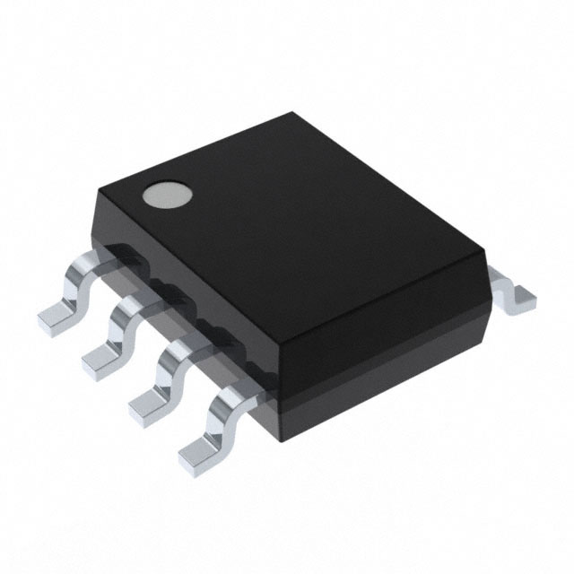
The MAX988ESA is a general-purpose comparator IC manufactured by Analog Devices Inc./Maxim Integrated, housed in an 8-SOIC surface-mount package. This device features open-drain output configuration and operates across single or dual supply voltages (2.5V ~ 5.5V or ±1.25V ~ 2.75V). The MAX988ESA is classified as obsolete, making identification of functionally equivalent alternatives essential for ongoing design support and production continuity.
Substiute Parts
Key Parameters
| Parameter | Value |
|---|---|
| Manufacturer Part Number | MAX988ESA |
| Manufacturer | Analog Devices Inc./Maxim Integrated |
| Category | Linear |
| Description | IC COMPARATOR 1 GEN PUR 8SOIC |
| Type | General Purpose |
| Output Type | Open-Drain |
| Voltage - Supply, Single/Dual (±) | 2.5V ~ 5.5V, ±1.25V ~ 2.75V |
| Voltage - Input Offset (Max) | 5mV @ 5.5V |
| Current - Input Bias (Max) | 1pA @ 5.5V |
| Current - Quiescent (Max) | 96µA |
| CMRR, PSRR (Typ) | 80dB CMRR, 80dB PSRR |
| Propagation Delay (Max) | 210ns |
| Hysteresis | ±2.5mV |
| Operating Temperature | -40°C ~ 85°C |
| Package / Case | 8-SOIC (0.154", 3.90mm Width) |
| Mounting Type | Surface Mount |
| Product Status | Obsolete |
| RoHS Status | ROHS3 Compliant |
| MSL | 1 (Unlimited) |
Substitute Part Grouping Explanation
Substitution eligibility for the MAX988ESA is determined by the following critical parameters:
Electrical Compatibility Requirements:
- Output Type: Open-Drain configuration
- Supply Voltage Range: Minimum coverage of 2.5V ~ 5.5V or ±1.25V ~ 2.75V
- Input Offset Voltage: Maximum 5mV @ rated voltage
- Input Bias Current: Maximum 1pA @ rated voltage
- Quiescent Current: Maximum 96µA
- CMRR/PSRR: Minimum 80dB for both metrics
- Propagation Delay: Maximum 210ns
- Hysteresis: ±2.5mV tolerance
Mechanical Compatibility Requirements:
- Package Type: 8-SOIC or compatible footprint
- Mounting Type: Surface Mount
- Pin count and pitch compatibility
Compliance Requirements:
- RoHS3 Compliant
- MSL Level 1 (Unlimited)
Two substitute parts meet these criteria with varying degrees of parameter alignment and package considerations.
Parameter Comparison
| Parameter | MAX988ESA (Main) | MAX988ESA+ (Direct) | NCS2202SQ2T2G (Alternative) |
|---|---|---|---|
| Manufacturer | Analog Devices Inc./Maxim Integrated | Analog Devices Inc./Maxim Integrated | onsemi |
| Product Status | Obsolete | Active | Active |
| Type | General Purpose | General Purpose | General Purpose |
| Output Type | Open-Drain | Open-Drain | Open-Drain, Rail-to-Rail |
| Voltage - Supply, Single/Dual (±) | 2.5V ~ 5.5V, ±1.25V ~ 2.75V | 2.5V ~ 5.5V, ±1.25V ~ 2.75V | 0.85V ~ 6V |
| Voltage - Input Offset (Max) | 5mV @ 5.5V | 5mV @ 5.5V | 5mV @ 6V |
| Current - Input Bias (Max) | 1pA @ 5.5V | 1pA @ 5.5V | 1pA @ 6V |
| Current - Quiescent (Max) | 96µA | 96µA | 17µA |
| CMRR, PSRR (Typ) | 80dB CMRR, 80dB PSRR | 80dB CMRR, 80dB PSRR | 70dB CMRR, 80dB PSRR |
| Propagation Delay (Max) | 210ns | 210ns | 1.1µs |
| Hysteresis | ±2.5mV | ±2.5mV | 20mV |
| Operating Temperature | -40°C ~ 85°C | -40°C ~ 85°C | -40°C ~ 105°C |
| Package / Case | 8-SOIC (0.154", 3.90mm Width) | 8-SOIC (0.154", 3.90mm Width) | 5-TSSOP, SC-70-5, SOT-353 |
| Mounting Type | Surface Mount | Surface Mount | Surface Mount |
| RoHS Status | ROHS3 Compliant | ROHS3 Compliant | ROHS3 Compliant |
| MSL | 1 (Unlimited) | 1 (Unlimited) | 1 (Unlimited) |
Engineering Selection Recommendations
MAX988ESA+ (Direct Substitute)
The MAX988ESA+ is the primary equivalent for the obsolete MAX988ESA. Both parts share identical electrical specifications, including supply voltage range, input offset voltage, input bias current, quiescent current, CMRR/PSRR ratings, propagation delay, and hysteresis characteristics. The MAX988ESA+ maintains the same 8-SOIC package footprint, ensuring direct PCB compatibility without layout modifications. The critical distinction is product status: MAX988ESA+ is active and currently in production, with 909 units in stock. Both parts are ROHS3 compliant with MSL Level 1 rating. Selection of MAX988ESA+ eliminates obsolescence risk while preserving all electrical and mechanical design parameters.
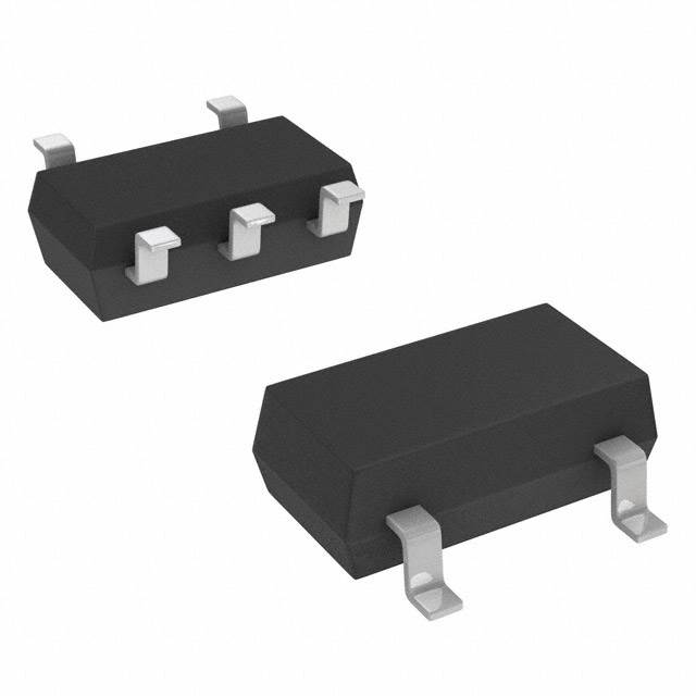
NCS2202SQ2T2G (Alternative Substitute)
The NCS2202SQ2T2G, manufactured by onsemi, provides functional equivalence with notable parameter deviations and package differences. This device meets the open-drain output requirement and maintains input offset voltage and input bias current specifications. However, the NCS2202SQ2T2G exhibits lower quiescent current (17µA versus 96µA), reduced CMRR (70dB versus 80dB), extended propagation delay (1.1µs versus 210ns), and increased hysteresis (20mV versus ±2.5mV). The supply voltage range is broader (0.85V ~ 6V), and operating temperature extends to 105°C. The package differs significantly: 5-TSSOP/SC-70-5/SOT-353 versus 8-SOIC, requiring PCB redesign and layout modifications. Selection of NCS2202SQ2T2G is appropriate only when package constraints or extended temperature operation are design requirements, and when the parameter differences do not compromise application performance.
Frequently Asked Questions (FAQ)
Q: Can MAX988ESA+ be used as a direct replacement for MAX988ESA?
A: Yes. The MAX988ESA+ is electrically and mechanically identical to the MAX988ESA. Both parts feature the same 8-SOIC package, identical supply voltage range (2.5V ~ 5.5V or ±1.25V ~ 2.75V), and matching electrical specifications including 5mV input offset voltage, 1pA input bias current, 96µA quiescent current, 80dB CMRR/PSRR, 210ns propagation delay, and ±2.5mV hysteresis. No circuit modifications or PCB layout changes are required. The MAX988ESA+ is currently in active production status.
Q: What are the key differences between MAX988ESA and NCS2202SQ2T2G?
A: The primary differences are package type and electrical performance. The NCS2202SQ2T2G uses a 5-TSSOP/SC-70-5/SOT-353 package instead of 8-SOIC, requiring PCB redesign. Electrically, the NCS2202SQ2T2G has lower quiescent current (17µA), reduced CMRR (70dB), slower propagation delay (1.1µs), and higher hysteresis (20mV). The NCS2202SQ2T2G offers broader supply voltage range (0.85V ~ 6V) and extended operating temperature (-40°C ~ 105°C).
Q: Is the NCS2202SQ2T2G suitable for high-speed applications?
A: The NCS2202SQ2T2G has a maximum propagation delay of 1.1µs, compared to 210ns for the MAX988ESA. For applications requiring fast response times, the MAX988ESA or MAX988ESA+ is the appropriate choice. The NCS2202SQ2T2G is suitable for general-purpose comparator applications where propagation delay is not a critical constraint.
Q: Can I use NCS2202SQ2T2G without modifying my PCB?
A: No. The NCS2202SQ2T2G uses a 5-TSSOP/SC-70-5/SOT-353 package, which has a different footprint than the 8-SOIC package of the MAX988ESA. PCB layout modifications are required, including new pad patterns and trace routing adjustments.
Q: Are all three parts RoHS3 compliant?
A: Yes. The MAX988ESA, MAX988ESA+, and NCS2202SQ2T2G are all ROHS3 compliant with MSL Level 1 (Unlimited) moisture sensitivity rating.
Q: Which substitute should I select for a new design?
A: For new designs, the MAX988ESA+ is the recommended choice. It provides identical electrical and mechanical specifications to the obsolete MAX988ESA, ensuring compatibility with existing design documentation and PCB layouts. The MAX988ESA+ is in active production with adequate inventory availability. The NCS2202SQ2T2G should be selected only when specific design constraints (such as package size reduction or extended temperature operation) justify the electrical performance trade-offs and PCB redesign effort.
Alternative Parts

SJ6012L2TP
Littelfuse Inc.
6 Alternative Parts

JMK107BBJ476MA-RE
Taiyo Yuden
10 Alternative Parts

GMK107BBJ475MA-T
Taiyo Yuden
5 Alternative Parts
SJ6020N2ARP
Littelfuse Inc.
3 Alternative Parts
SJ6025R2ATP
Littelfuse Inc.
4 Alternative Parts

2474-05L
API Delevan Inc.
1 Alternative Parts

4590R-684K
API Delevan Inc.
1 Alternative Parts

CM6560R-334
API Delevan Inc.
1 Alternative Parts

CM6460-104
API Delevan Inc.
1 Alternative Parts

5526-12
API Delevan Inc.
1 Alternative Parts