


Request Quote
(Ships tomorrow)
MAX907C/D Equivalent & Substitute Parts
Part Overview
The MAX907C/D is a general-purpose comparator IC featuring 2 elements with TTL output, manufactured by Analog Devices Inc./Maxim Integrated. This component is supplied as a die in surface mount configuration and is classified as obsolete. The obsolete status necessitates identification of active equivalent parts to maintain design continuity and ensure long-term component availability for production and maintenance applications.
Substiute Parts
Key Parameters
| Parameter | Value |
|---|---|
| Manufacturer Part Number | MAX907C/D |
| Manufacturer | Analog Devices Inc./Maxim Integrated |
| Category | Linear |
| Type | General Purpose Comparator |
| Number of Elements | 2 |
| Output Type | TTL |
| Voltage - Supply, Single/Dual (±) | 4.5V ~ 5.5V |
| Voltage - Input Offset (Max) | 2mV @ 5V |
| Current - Input Bias (Max) | 0.3µA @ 5V |
| Current - Quiescent (Max) | 1mA |
| CMRR, PSRR (Typ) | 34dB CMRR, 34dB PSRR |
| Propagation Delay (Max) | 50ns |
| Operating Temperature | 0°C ~ 70°C |
| Package / Case | Die |
| Mounting Type | Surface Mount |
| Product Status | Obsolete |
| RoHS Status | ROHS3 Compliant |
| Moisture Sensitivity Level (MSL) | 1 (Unlimited) |
Substitute Part Grouping Explanation
Substitution of the MAX907C/D is determined by the following critical parameters that must remain consistent across equivalent parts:
- Functional equivalence: 2-element general-purpose comparator with TTL output
- Electrical specifications: Input offset voltage (2mV @ 5V), input bias current (0.3µA @ 5V), quiescent current (1mA), and propagation delay (50ns)
- Supply voltage compatibility: Operating range must accommodate the original 4.5V ~ 5.5V specification
- Temperature range: 0°C ~ 70°C operating temperature
- Compliance requirements: ROHS3 compliance and MSL 1 rating
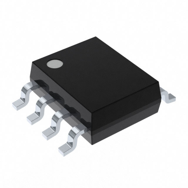
The MAX907CSA+ qualifies as a direct substitute based on matching functional type, electrical performance characteristics, and compliance certifications. The primary distinction is packaging format: the substitute transitions from die form to 8-SOIC surface mount package, which expands supply voltage capability to 4.5V ~ 11V while maintaining all critical electrical parameters.
Parameter Comparison
| Parameter | MAX907C/D | MAX907CSA+ |
|---|---|---|
| Manufacturer | Analog Devices Inc./Maxim Integrated | Analog Devices Inc./Maxim Integrated |
| Type | General Purpose Comparator | General Purpose Comparator |
| Number of Elements | 2 | 2 |
| Output Type | TTL | TTL |
| Voltage - Supply, Single/Dual (±) | 4.5V ~ 5.5V | 4.5V ~ 11V |
| Voltage - Input Offset (Max) | 2mV @ 5V | 2mV @ 5V |
| Current - Input Bias (Max) | 0.3µA @ 5V | 0.3µA @ 5V |
| Current - Quiescent (Max) | 1mA | 1mA |
| Propagation Delay (Max) | 50ns | 50ns |
| Operating Temperature | 0°C ~ 70°C | 0°C ~ 70°C |
| Package / Case | Die | 8-SOIC (0.154", 3.90mm Width) |
| Mounting Type | Surface Mount | Surface Mount |
| Product Status | Obsolete | Active |
| RoHS Status | ROHS3 Compliant | ROHS3 Compliant |
| Moisture Sensitivity Level (MSL) | 1 (Unlimited) | 1 (Unlimited) |
Engineering Selection Recommendations
The MAX907CSA+ is the designated manufacturer-recommended substitute for the obsolete MAX907C/D. Selection of this substitute is supported by the following factors:
- Active product status: The MAX907CSA+ maintains active production status, ensuring long-term availability and supply chain continuity.
- Compliance alignment: Both parts maintain ROHS3 compliance and identical MSL ratings, satisfying regulatory and environmental requirements.
- Electrical parameter equivalence: All critical electrical specifications—input offset voltage, input bias current, quiescent current, and propagation delay—remain unchanged, ensuring functional compatibility within existing circuit designs.
- Enhanced supply voltage range: The substitute accommodates an expanded supply voltage range (4.5V ~ 11V) compared to the original specification (4.5V ~ 5.5V), providing additional design flexibility without compromising performance at the original operating voltage.
- Package transition: Migration from die form to 8-SOIC package format enables standard surface mount assembly processes and improves handling and integration into production workflows.
Frequently Asked Questions (FAQ)
Q: Can the MAX907CSA+ directly replace the MAX907C/D in existing designs?
A: Yes. The MAX907CSA+ maintains electrical equivalence across all specified parameters including input offset voltage, input bias current, quiescent current, and propagation delay. The primary design consideration is the package format transition from die to 8-SOIC, which requires PCB layout modification but does not affect electrical performance.
Q: What is the significance of the expanded supply voltage range in the MAX907CSA+?
A: The MAX907CSA+ operates across 4.5V ~ 11V, compared to the original 4.5V ~ 5.5V specification. This expanded range provides additional design margin and flexibility for applications requiring higher supply voltages. Designs operating within the original 4.5V ~ 5.5V window experience no performance change.
Q: Are there compliance or certification differences between the two parts?
A: No. Both the MAX907C/D and MAX907CSA+ maintain identical ROHS3 compliance status and MSL 1 ratings. No additional compliance verification is required for substitution.
Q: How does the package change from die to 8-SOIC affect circuit implementation?
A: The transition from die form to 8-SOIC package requires PCB layout redesign to accommodate the 8-pin surface mount footprint. Electrical functionality and pin configuration remain equivalent. Standard surface mount assembly processes apply to the MAX907CSA+.
Q: Is the MAX907CSA+ the only available substitute?
A: Based on the provided manufacturer data, the MAX907CSA+ is the designated manufacturer-recommended substitute. This part maintains the same base product number (MAX907) and functional classification as the obsolete MAX907C/D.
Alternative Parts

SJ6012L2TP
Littelfuse Inc.
6 Alternative Parts

JMK107BBJ476MA-RE
Taiyo Yuden
10 Alternative Parts

GMK107BBJ475MA-T
Taiyo Yuden
5 Alternative Parts
SJ6020N2ARP
Littelfuse Inc.
3 Alternative Parts
SJ6025R2ATP
Littelfuse Inc.
4 Alternative Parts

2474-05L
API Delevan Inc.
1 Alternative Parts

4590R-684K
API Delevan Inc.
1 Alternative Parts

CM6560R-334
API Delevan Inc.
1 Alternative Parts

CM6460-104
API Delevan Inc.
1 Alternative Parts

5526-12
API Delevan Inc.
1 Alternative Parts