


Request Quote
(Ships tomorrow)
MAX4462TESA Equivalent & Substitute Parts
Part Overview
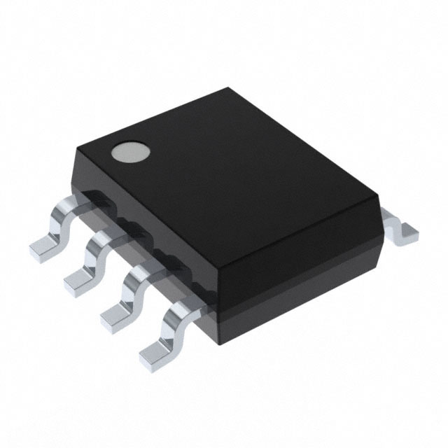
The MAX4462TESA is a single-channel instrumentation amplifier manufactured by Analog Devices Inc./Maxim Integrated, housed in an 8-SOIC surface mount package. This device features rail-to-rail output capability and is designed for precision signal conditioning applications requiring low input offset voltage and minimal input bias current.
The MAX4462TESA is classified as obsolete. Identifying equivalent and substitute parts is necessary to ensure design continuity, maintain supply chain reliability, and support long-term product availability for applications currently utilizing this component.
Substiute Parts
Key Parameters
| Parameter | Value | Unit |
|---|---|---|
| Amplifier Type | Instrumentation | — |
| Number of Circuits | 1 | — |
| Output Type | Rail-to-Rail | — |
| Slew Rate | 0.5 | V/µs |
| Gain Bandwidth Product | 2.5 | MHz |
| -3dB Bandwidth | 250 | kHz |
| Current - Input Bias | 1 | pA |
| Voltage - Input Offset | 100 | µV |
| Current - Supply | 800 | µA |
| Current - Output / Channel | 150 | mA |
| Voltage - Supply Span (Min) | 2.85 | V |
| Voltage - Supply Span (Max) | 5.25 | V |
| Operating Temperature Range | -40 to 85 | °C |
| Package / Case | 8-SOIC (0.154", 3.90mm Width) | — |
| Mounting Type | Surface Mount | — |
Substitute Part Grouping Explanation
Substitution eligibility for the MAX4462TESA is determined by strict equivalence across the following critical parameters:
Functional Parameters:
- Amplifier type: Instrumentation
- Number of circuits: 1
- Output type: Rail-to-Rail
- Slew rate: 0.5 V/µs
- Gain bandwidth product: 2.5 MHz
- -3dB bandwidth: 250 kHz
- Input bias current: 1 pA
- Supply current: 800 µA
- Output current per channel: 150 mA
- Supply voltage range: 2.85 V to 5.25 V
- Operating temperature range: -40°C to 85°C
Package & Mechanical Parameters:
- Package type: 8-SOIC
- Mounting type: Surface Mount
- Physical dimensions: 0.154" width (3.90mm)
The MAX4461TESA+ meets all functional and mechanical equivalence criteria. Differences in input offset voltage (50 µV vs. 100 µV) and product status (Active vs. Obsolete) do not disqualify substitution but represent improvements in the substitute part.
Parameter Comparison
| Parameter | MAX4462TESA | MAX4461TESA+ | Match |
|---|---|---|---|
| Amplifier Type | Instrumentation | Instrumentation | ✓ |
| Number of Circuits | 1 | 1 | ✓ |
| Output Type | Rail-to-Rail | Rail-to-Rail | ✓ |
| Slew Rate (V/µs) | 0.5 | 0.5 | ✓ |
| Gain Bandwidth Product (MHz) | 2.5 | 2.5 | ✓ |
| -3dB Bandwidth (kHz) | 250 | 250 | ✓ |
| Current - Input Bias (pA) | 1 | 1 | ✓ |
| Voltage - Input Offset (µV) | 100 | 50 | Improved |
| Current - Supply (µA) | 800 | 800 | ✓ |
| Current - Output / Channel (mA) | 150 | 150 | ✓ |
| Voltage - Supply Span Min (V) | 2.85 | 2.85 | ✓ |
| Voltage - Supply Span Max (V) | 5.25 | 5.25 | ✓ |
| Operating Temperature (°C) | -40 to 85 | -40 to 85 | ✓ |
| Package / Case | 8-SOIC (0.154", 3.90mm) | 8-SOIC (0.154", 3.90mm) | ✓ |
| Mounting Type | Surface Mount | Surface Mount | ✓ |
| Product Status | Obsolete | Active | — |
| RoHS Status | Non-compliant | ROHS3 Compliant | — |
Engineering Selection Recommendations
MAX4461TESA+ as Primary Substitute:
The MAX4461TESA+ is a direct functional and mechanical equivalent to the MAX4462TESA. All critical electrical parameters—slew rate, gain bandwidth product, bandwidth, input bias current, supply current, output current, and supply voltage range—are identical. Both devices operate across the same temperature range and use identical 8-SOIC surface mount packaging.
The MAX4461TESA+ offers two significant advantages:
-
Product Status: The MAX4461TESA+ is classified as Active, ensuring ongoing manufacturer support, continued availability, and access to technical documentation and design resources.
-
Regulatory Compliance: The MAX4461TESA+ is ROHS3 compliant, meeting current environmental and regulatory requirements for new designs and procurement. The MAX4462TESA is RoHS non-compliant.
The input offset voltage of the MAX4461TESA+ (50 µV) is superior to the MAX4462TESA (100 µV), representing an improvement in precision performance. This difference does not prevent substitution and may enhance system accuracy in applications sensitive to input offset.
Substitution Compatibility:
Direct pin-for-pin and functional substitution is supported. No circuit modifications, PCB layout changes, or firmware updates are required. The identical package footprint and pinout ensure mechanical and electrical compatibility.
Frequently Asked Questions (FAQ)
Q: Can the MAX4461TESA+ be used as a direct replacement for the MAX4462TESA in existing designs?
A: Yes. The MAX4461TESA+ is functionally and mechanically equivalent. All electrical parameters critical to circuit operation are identical, including slew rate, bandwidth, input bias current, and supply voltage range. The identical 8-SOIC package ensures pin-for-pin compatibility without PCB modifications.
Q: What is the difference in input offset voltage between these parts?
A: The MAX4462TESA specifies a maximum input offset voltage of 100 µV, while the MAX4461TESA+ specifies 50 µV. This represents improved precision in the substitute part. For applications where input offset voltage is a critical parameter, the MAX4461TESA+ provides superior performance.
Q: Why is the MAX4462TESA classified as obsolete?
A: The MAX4462TESA is listed as obsolete by the manufacturer. The MAX4461TESA+ is the active equivalent product. Obsolete status indicates that the manufacturer no longer produces the part and may have limited or no remaining inventory. Transitioning to the MAX4461TESA+ ensures long-term design support and supply chain continuity.
Q: Are there any compliance differences between these parts?
A: Yes. The MAX4461TESA+ is ROHS3 compliant, meeting current environmental regulations. The MAX4462TESA is RoHS non-compliant. For new designs or procurement subject to RoHS requirements, the MAX4461TESA+ is the appropriate choice.
Q: Is the packaging identical between these parts?
A: Yes. Both the MAX4462TESA and MAX4461TESA+ use the 8-SOIC package with 0.154" width (3.90mm). The physical dimensions, pin spacing, and surface mount footprint are identical. No PCB layout modifications are required for substitution.
Q: What is the supply voltage range for both parts?
A: Both the MAX4462TESA and MAX4461TESA+ operate across a supply voltage range of 2.85 V to 5.25 V. This range supports single-supply and dual-supply configurations within the specified limits.
Q: Are there any temperature range limitations?
A: Both parts operate across the same temperature range: -40°C to 85°C. No thermal performance differences exist between the two devices.
Alternative Parts

SJ6012L2TP
Littelfuse Inc.
6 Alternative Parts

JMK107BBJ476MA-RE
Taiyo Yuden
10 Alternative Parts

GMK107BBJ475MA-T
Taiyo Yuden
5 Alternative Parts
SJ6020N2ARP
Littelfuse Inc.
3 Alternative Parts
SJ6025R2ATP
Littelfuse Inc.
4 Alternative Parts

2474-05L
API Delevan Inc.
1 Alternative Parts

4590R-684K
API Delevan Inc.
1 Alternative Parts

CM6560R-334
API Delevan Inc.
1 Alternative Parts

CM6460-104
API Delevan Inc.
1 Alternative Parts

5526-12
API Delevan Inc.
1 Alternative Parts