


Request Quote
(Ships tomorrow)
MAX4287ESA Equivalent & Substitute Parts
Part Overview
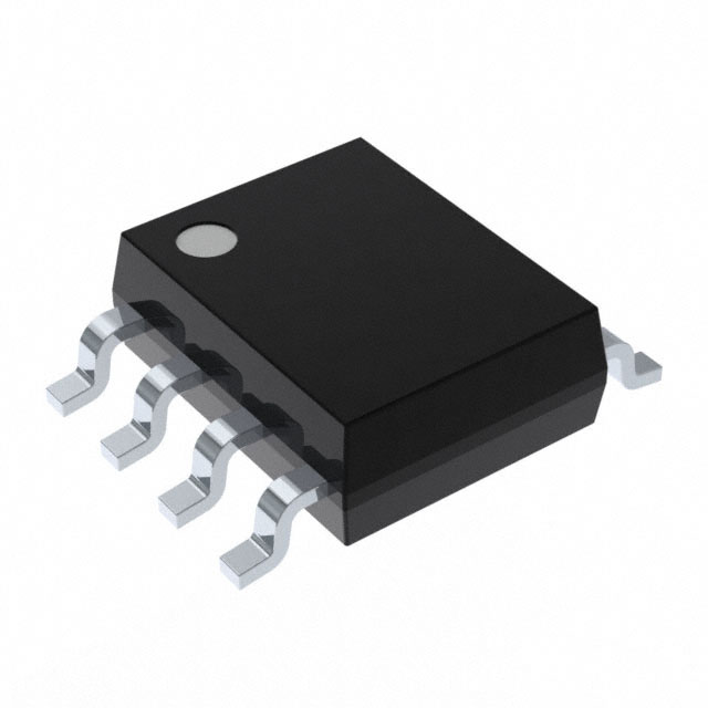
The MAX4287ESA is a buffer and voltage feedback amplifier integrated circuit manufactured by Analog Devices Inc./Maxim Integrated. This device contains 2 circuits in an 8-SOIC surface mount package and is designed for applications requiring high-speed buffering and amplification. The MAX4287ESA is classified as obsolete, making identification of functionally equivalent substitute components necessary for ongoing design support, maintenance, and new production requirements.
Substiute Parts
Key Parameters
| Parameter | Value | Unit |
|---|---|---|
| Amplifier Type | Buffer, Voltage Feedback | — |
| Number of Circuits | 2 | — |
| Slew Rate | 385 | V/µs |
| -3dB Bandwidth | 250 | MHz |
| Current - Input Bias | 13 | µA |
| Voltage - Input Offset | 100 | µV |
| Current - Supply (per Channel) | 23 | mA |
| Current - Output / Channel | 106 | mA |
| Voltage - Supply Span (Min) | 2.85 | V |
| Voltage - Supply Span (Max) | 6.5 | V |
| Operating Temperature Range | -40 to 85 | °C |
| Package / Case | 8-SOIC (0.154", 3.90mm Width) | — |
| Mounting Type | Surface Mount | — |
| Product Status | Obsolete | — |
| RoHS Status | RoHS non-compliant | — |
Substitute Part Grouping Explanation
Substitution of the MAX4287ESA is determined by the following critical parameters that must be matched or exceeded:
Package Compatibility: Both the main part and substitute must use the 8-SOIC surface mount package with identical pinout configuration to ensure direct PCB compatibility without layout modifications.
Circuit Count: The substitute must contain 2 circuits to maintain functional equivalence in dual-channel applications.
Operating Temperature Range: The substitute must support the full -40°C to 85°C operating temperature range specified for the MAX4287ESA.
Supply Voltage Range: The substitute must operate within or encompass the 2.85 V to 6.5 V supply voltage span of the original part.
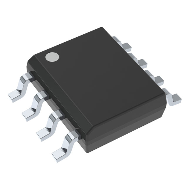
Electrical Performance: While the substitute may differ in specific performance metrics such as slew rate, bandwidth, and input bias current, these parameters must be suitable for the intended application. The substitute TLV2322IDR operates within compatible electrical specifications for buffer and amplifier applications, though with different performance characteristics reflecting its CMOS architecture versus the original bipolar design.
Parameter Comparison
| Parameter | MAX4287ESA | TLV2322IDR | Unit |
|---|---|---|---|
| Manufacturer | Analog Devices Inc./Maxim Integrated | Texas Instruments | — |
| Amplifier Type | Buffer, Voltage Feedback | CMOS | — |
| Number of Circuits | 2 | 2 | — |
| Slew Rate | 385 | 0.03 | V/µs |
| Current - Input Bias | 13 | 0.6 | µA |
| Voltage - Input Offset | 100 | 1.1 | mV |
| Current - Supply (per Channel) | 23 | 20 | µA |
| Current - Output / Channel | 106 | 30 | mA |
| Voltage - Supply Span (Min) | 2.85 | 2 | V |
| Voltage - Supply Span (Max) | 6.5 | 8 | V |
| Operating Temperature Range | -40 to 85 | -40 to 85 | °C |
| Package / Case | 8-SOIC (0.154", 3.90mm Width) | 8-SOIC (0.154", 3.90mm Width) | — |
| Mounting Type | Surface Mount | Surface Mount | — |
| Product Status | Obsolete | Active | — |
| RoHS Status | RoHS non-compliant | ROHS3 Compliant | — |
| Moisture Sensitivity Level (MSL) | 1 (Unlimited) | 1 (Unlimited) | — |
Engineering Selection Recommendations
Product Status Consideration: The MAX4287ESA is classified as obsolete, while the TLV2322IDR is active and in production. Selection of the TLV2322IDR as a substitute ensures access to current inventory and ongoing manufacturing support.
Compliance Status: The TLV2322IDR is ROHS3 compliant, whereas the MAX4287ESA is RoHS non-compliant. For applications subject to RoHS regulations or environmental compliance requirements, the TLV2322IDR provides regulatory alignment.
Package and Pinout Compatibility: Both devices use identical 8-SOIC surface mount packaging with 0.154" width and 3.90mm dimensions. Direct PCB substitution is possible without layout modifications.
Electrical Performance Trade-offs: The TLV2322IDR exhibits significantly lower slew rate (0.03 V/µs versus 385 V/µs) and reduced output current capability (30 mA versus 106 mA per channel). Applications requiring high-speed transient response or high output current drive must evaluate whether the TLV2322IDR performance is acceptable for the specific circuit requirements.
Supply Voltage Range: The TLV2322IDR operates across a wider supply voltage range (2 V to 8 V) compared to the MAX4287ESA (2.85 V to 6.5 V), providing greater flexibility in power supply design.
Frequently Asked Questions (FAQ)
Q: Can the TLV2322IDR be used as a direct replacement for the MAX4287ESA without circuit modifications?
A: The TLV2322IDR shares the same 8-SOIC package and pinout, allowing direct PCB substitution. However, the significantly different electrical performance characteristics—particularly slew rate and output current—require circuit-level evaluation to confirm functional compatibility with the specific application.
Q: What are the primary differences between the MAX4287ESA and TLV2322IDR?
A: The MAX4287ESA is a bipolar buffer/voltage feedback amplifier with high slew rate (385 V/µs) and high output current (106 mA per channel). The TLV2322IDR is a CMOS amplifier with lower slew rate (0.03 V/µs) and reduced output current (30 mA per channel). The TLV2322IDR offers lower input bias current and lower supply current, making it suitable for low-power applications.
Q: Is the TLV2322IDR suitable for high-frequency applications?
A: The TLV2322IDR has a gain bandwidth product of 85 kHz, which is significantly lower than the MAX4287ESA's -3dB bandwidth of 250 MHz. Applications requiring high-frequency response should verify that the TLV2322IDR bandwidth is adequate for the intended use.
Q: What is the impact of the lower slew rate in the TLV2322IDR?
A: The TLV2322IDR's slew rate of 0.03 V/µs limits the rate of voltage change at the output. Applications requiring fast transient response or high-speed signal buffering may not be suitable for the TLV2322IDR. Slew rate requirements should be evaluated against the specific circuit demands.
Q: Are there any compliance advantages to using the TLV2322IDR?
A: The TLV2322IDR is ROHS3 compliant, whereas the MAX4287ESA is RoHS non-compliant. For applications subject to RoHS directives or environmental regulations, the TLV2322IDR provides regulatory compliance. Both devices have MSL 1 (Unlimited) moisture sensitivity ratings.
Q: What is the difference in supply current between these devices?
A: The MAX4287ESA draws 23 mA per channel, while the TLV2322IDR draws 20 µA per channel. The TLV2322IDR's significantly lower supply current makes it advantageous for battery-powered or low-power applications.
Q: Can the TLV2322IDR handle the same output current as the MAX4287ESA?
A: No. The MAX4287ESA provides 106 mA per channel output current, while the TLV2322IDR provides only 30 mA per channel. Applications requiring high output current drive must confirm that 30 mA is sufficient for the load impedance and signal levels in the circuit.
Q: Are both devices available in the same packaging format?
A: Yes. Both the MAX4287ESA and TLV2322IDR use 8-SOIC surface mount packaging with identical dimensions (0.154" width, 3.90mm). The TLV2322IDR is supplied in Tape & Reel (TR) packaging format.
Alternative Parts

SJ6012L2TP
Littelfuse Inc.
6 Alternative Parts

JMK107BBJ476MA-RE
Taiyo Yuden
10 Alternative Parts

GMK107BBJ475MA-T
Taiyo Yuden
5 Alternative Parts
SJ6020N2ARP
Littelfuse Inc.
3 Alternative Parts
SJ6025R2ATP
Littelfuse Inc.
4 Alternative Parts

2474-05L
API Delevan Inc.
1 Alternative Parts

4590R-684K
API Delevan Inc.
1 Alternative Parts

CM6560R-334
API Delevan Inc.
1 Alternative Parts

CM6460-104
API Delevan Inc.
1 Alternative Parts

5526-12
API Delevan Inc.
1 Alternative Parts