


Request Quote
(Ships tomorrow)
MAX397CWI Equivalent & Substitute Parts
Part Overview
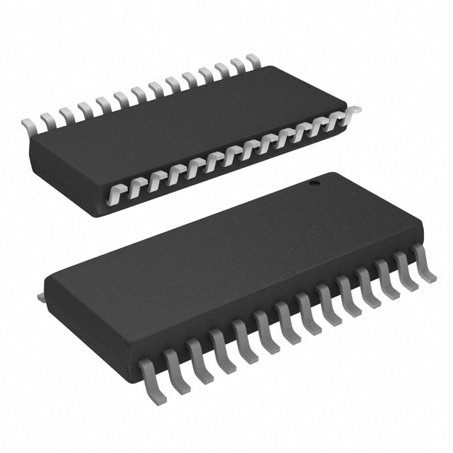
The MAX397CWI is a dual 8:1 analog multiplexer/demultiplexer IC manufactured by Analog Devices Inc./Maxim Integrated. This component features two independent 8:1 switch circuits with 100Ohm on-state resistance in a 28-SOIC surface mount package. The MAX397CWI is classified as obsolete, making identification of compatible substitute parts essential for ongoing system support and new design implementations.
Substiute Parts
Key Parameters
| Parameter | Value |
|---|---|
| Multiplexer/Demultiplexer Circuit Configuration | 8:1 |
| Number of Circuits | 2 |
| On-State Resistance (Max) | 100Ohm |
| Channel-to-Channel Matching (ΔRon) | 1.8Ohm |
| Voltage - Supply, Single (V+) | 2.7V ~ 16V |
| Voltage - Supply, Dual (V±) | ±2.7V ~ 8V |
| Switch Time (Ton, Toff) (Max) | 150ns, 150ns |
| Charge Injection | 2pC |
| Channel Capacitance (CS(off), CD(off)) | 11pF, 80pF |
| Current - Leakage (IS(off)) (Max) | 100pA |
| Crosstalk | -92dB @ 100kHz |
| Operating Temperature | 0°C ~ 70°C |
| Package / Case | 28-SOIC (0.295", 7.50mm Width) |
| Mounting Type | Surface Mount |
Substitute Part Grouping Explanation
Substitution of the MAX397CWI is determined by strict equivalence across the following critical parameters:
Multiplexer configuration (8:1 dual circuit architecture), on-state resistance specification (100Ohm maximum), package form factor (28-SOIC), and mounting type (surface mount). The DG407EWI+ meets these core functional and mechanical requirements.
Additional parameters that define substitution compatibility include supply voltage ranges, switch timing characteristics, charge injection, channel capacitance, leakage current, and crosstalk performance. While the DG407EWI+ operates within different voltage ranges and exhibits variations in secondary electrical characteristics, it maintains the primary functional specification of a dual 8:1 multiplexer with 100Ohm on-state resistance in the identical package.
Parameter Comparison
| Parameter | MAX397CWI | DG407EWI+ |
|---|---|---|
| Multiplexer/Demultiplexer Circuit | 8:1 | 8:1 |
| Number of Circuits | 2 | 2 |
| On-State Resistance (Max) | 100Ohm | 100Ohm |
| Channel-to-Channel Matching (ΔRon) | 1.8Ohm | 1.5Ohm |
| Voltage - Supply, Single (V+) | 2.7V ~ 16V | 5V ~ 30V |
| Voltage - Supply, Dual (V±) | ±2.7V ~ 8V | ±4.5V ~ 20V |
| Switch Time Ton (Max) | 150ns | 200ns |
| Switch Time Toff (Max) | 150ns | 150ns |
| Charge Injection | 2pC | 2pC |
| Channel Capacitance CS(off) | 11pF | 8pF |
| Channel Capacitance CD(off) | 80pF | 65pF |
| Current - Leakage (IS(off)) (Max) | 100pA | 500pA |
| Crosstalk | -92dB @ 100kHz | -92dB @ 100kHz |
| Operating Temperature | 0°C ~ 70°C | -40°C ~ 85°C |
| Package / Case | 28-SOIC | 28-SOIC |
| Mounting Type | Surface Mount | Surface Mount |
| Product Status | Obsolete | Active |
| RoHS Status | RoHS non-compliant | ROHS3 Compliant |
Engineering Selection Recommendations
The DG407EWI+ is the manufacturer-recommended substitute for the obsolete MAX397CWI. Both devices share identical multiplexer architecture (dual 8:1), on-state resistance (100Ohm maximum), and 28-SOIC package specifications, establishing functional and mechanical compatibility.
The DG407EWI+ offers extended operating temperature range (-40°C to 85°C versus 0°C to 70°C), improved RoHS3 compliance status, and active product availability. The DG407EWI+ exhibits tighter channel-to-channel matching (1.5Ohm versus 1.8Ohm) and reduced channel capacitance values, representing performance enhancements in the substitute design.
Design integration requires verification that the DG407EWI+ supply voltage requirements (5V ~ 30V single supply, ±4.5V ~ 20V dual supply) align with existing system power architecture. The MAX397CWI supports lower minimum supply voltages (2.7V single, ±2.7V dual), which may necessitate circuit redesign if ultra-low voltage operation is required. Switch time performance (200ns Ton maximum for DG407EWI+ versus 150ns for MAX397CWI) should be evaluated against system timing constraints.
Frequently Asked Questions (FAQ)
Q: Can the DG407EWI+ directly replace the MAX397CWI without PCB modifications?
A: Yes, the DG407EWI+ is pin-compatible and package-equivalent in the 28-SOIC form factor. No PCB layout changes are required for physical substitution. Circuit validation is necessary to confirm that supply voltage ranges and timing specifications align with system requirements.
Q: What are the primary electrical differences between these parts?
A: The DG407EWI+ operates at higher supply voltages (5V ~ 30V single supply versus 2.7V ~ 16V) and exhibits slower switch-on time (200ns versus 150ns). Leakage current is higher in the DG407EWI+ (500pA maximum versus 100pA). Channel capacitance values are lower in the substitute part, which may improve high-frequency performance in certain applications.
Q: Is the DG407EWI+ suitable for low-voltage applications below 5V?
A: No. The DG407EWI+ minimum single supply voltage is 5V. Applications requiring operation below 5V cannot use this substitute. Alternative parts with lower voltage specifications must be identified.
Q: What compliance advantages does the DG407EWI+ offer?
A: The DG407EWI+ is ROHS3 compliant, whereas the MAX397CWI is RoHS non-compliant. For applications subject to RoHS regulations, the DG407EWI+ provides regulatory compliance. Both parts are REACH Unaffected and carry EAR99 ECCN classification.
Q: How does the extended temperature range of the DG407EWI+ affect system design?
A: The DG407EWI+ operates from -40°C to 85°C, compared to the MAX397CWI range of 0°C to 70°C. This extended range supports industrial and automotive temperature environments without thermal derating. Systems operating within the narrower MAX397CWI range require no design changes.
Q: Are there inventory considerations for this substitution?
A: The MAX397CWI is obsolete with limited remaining stock (2060 pcs). The DG407EWI+ is an active product with current availability (1793 pcs in stock). Long-term supply chain planning should prioritize the DG407EWI+ for new designs and ongoing production.
Alternative Parts

SJ6012L2TP
Littelfuse Inc.
6 Alternative Parts

JMK107BBJ476MA-RE
Taiyo Yuden
10 Alternative Parts

GMK107BBJ475MA-T
Taiyo Yuden
5 Alternative Parts
SJ6020N2ARP
Littelfuse Inc.
3 Alternative Parts
SJ6025R2ATP
Littelfuse Inc.
4 Alternative Parts

2474-05L
API Delevan Inc.
1 Alternative Parts

4590R-684K
API Delevan Inc.
1 Alternative Parts

CM6560R-334
API Delevan Inc.
1 Alternative Parts

CM6460-104
API Delevan Inc.
1 Alternative Parts

5526-12
API Delevan Inc.
1 Alternative Parts