


Request Quote
(Ships tomorrow)
LP8340CLD-3.3/NOPB Equivalent & Substitute Parts
Part Overview
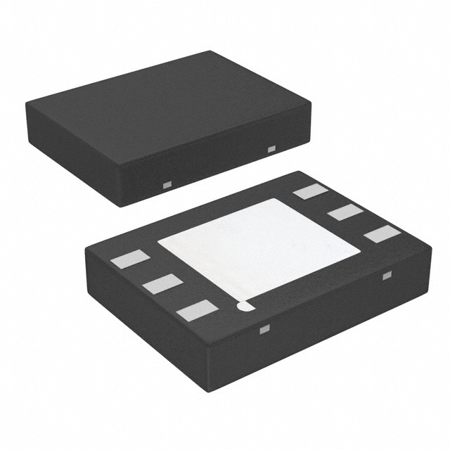
The LP8340CLD-3.3/NOPB is a linear voltage regulator IC manufactured by Texas Instruments, designed to deliver a fixed 3.3V output at 1A maximum current in a 6-WSON surface mount package. This device is classified as obsolete, making identification of functionally equivalent alternatives essential for ongoing design support and production continuity. The part provides positive fixed output regulation with integrated over-current and over-temperature protection suitable for low-power applications requiring stable 3.3V rails.
Substiute Parts
Key Parameters
| Parameter | Value |
|---|---|
| Manufacturer | Texas Instruments |
| Part Number | LP8340CLD-3.3/NOPB |
| Output Voltage (Fixed) | 3.3V |
| Output Current | 1A |
| Input Voltage (Max) | 10V |
| Voltage Dropout (Max) | 1V @ 1A |
| Quiescent Current | 100 µA |
| Package Type | 6-WSON (2.92x3.29) |
| Product Status | Obsolete |
| RoHS Compliance | ROHS3 Compliant |
Substitute Part Grouping Explanation
Substitution of the LP8340CLD-3.3/NOPB is determined by the following critical parameters:
- Fixed output voltage of 3.3V
- Maximum output current of 1A
- Surface mount packaging with exposed pad thermal management
- Positive fixed output configuration with single regulator
- Over-current and over-temperature protection features
- RoHS3 compliance and REACH unaffected status
The LD39100PU33R from STMicroelectronics meets these core functional requirements. Both devices deliver identical output voltage and current specifications, operate within compatible input voltage ranges, and provide equivalent protection mechanisms. The substitute part maintains RoHS3 and REACH compliance, ensuring regulatory alignment with the original component.
Parameter Comparison
| Parameter | LP8340CLD-3.3/NOPB (TI) | LD39100PU33R (STMicroelectronics) |
|---|---|---|
| Output Voltage | 3.3V Fixed | 3.3V Fixed |
| Output Current | 1A | 1A |
| Input Voltage (Max) | 10V | 5.5V |
| Voltage Dropout (Max) | 1V @ 1A | 0.4V @ 1A |
| Quiescent Current | 100 µA | 50 µA |
| Supply Current (Max) | 170 µA | 300 µA |
| PSRR | 55dB (120Hz) | 65dB ~ 62dB (1kHz ~ 10kHz) |
| Protection Features | Over Current, Over Temperature | Over Current, Over Temperature, Short Circuit |
| Operating Temperature | 0°C ~ 125°C | -40°C ~ 125°C (TJ) |
| Package Type | 6-WSON (2.92x3.29) | 6-DFN (3x3) |
| Product Status | Obsolete | Active |
| RoHS Status | ROHS3 Compliant | ROHS3 Compliant |
Engineering Selection Recommendations
The LD39100PU33R is the designated manufacturer-recommended substitute for the LP8340CLD-3.3/NOPB. Selection of this alternative is supported by:
- Active product status ensuring long-term availability and manufacturing support
- Identical output voltage and current specifications matching the original design requirements
- Superior voltage dropout performance (0.4V vs. 1V), reducing thermal dissipation in the regulator
- Lower quiescent current consumption (50 µA vs. 100 µA), improving system efficiency
- Enhanced protection features including short-circuit protection in addition to over-current and over-temperature functions
- Extended operating temperature range (-40°C to 125°C vs. 0°C to 125°C), providing broader environmental compatibility
- Maintained RoHS3 compliance and REACH unaffected status, preserving regulatory alignment
The primary design consideration is the reduced maximum input voltage specification (5.5V vs. 10V) on the substitute part. Applications operating with input voltages exceeding 5.5V require circuit redesign or alternative component selection.
Frequently Asked Questions (FAQ)
Q: Can the LD39100PU33R directly replace the LP8340CLD-3.3/NOPB in existing designs?
A: Direct replacement is possible for applications where the input voltage does not exceed 5.5V. The substitute part delivers identical output voltage and current, with improved dropout performance and additional protection features. Package dimensions differ (6-DFN 3x3 vs. 6-WSON 2.92x3.29), requiring PCB layout verification for pin-to-pin compatibility and thermal pad alignment.
Q: What are the key differences between these two regulators?
A: The LD39100PU33R provides superior performance characteristics including lower dropout voltage, reduced quiescent current, and additional short-circuit protection. The substitute part operates across a narrower input voltage range (5.5V maximum vs. 10V maximum) and supports an extended temperature range. Both devices maintain identical output specifications and regulatory compliance.
Q: Are there package compatibility concerns?
A: Yes. The LP8340CLD-3.3/NOPB uses a 6-WSON package (2.92x3.29mm), while the LD39100PU33R uses a 6-DFN package (3x3mm). Pin assignments and thermal pad locations differ. PCB redesign is required for mechanical and electrical compatibility, including trace routing and thermal management adjustments.
Q: Does the substitute part meet the same compliance requirements?
A: Yes. The LD39100PU33R maintains ROHS3 compliance and REACH unaffected status, matching the regulatory profile of the original component.
Q: What input voltage limitation should I consider?
A: The LD39100PU33R is rated for a maximum input voltage of 5.5V, compared to 10V for the LP8340CLD-3.3/NOPB. If your application requires input voltages above 5.5V, alternative component selection or circuit modification is necessary.
Alternative Parts

SJ6012L2TP
Littelfuse Inc.
6 Alternative Parts

JMK107BBJ476MA-RE
Taiyo Yuden
10 Alternative Parts

GMK107BBJ475MA-T
Taiyo Yuden
5 Alternative Parts
SJ6020N2ARP
Littelfuse Inc.
3 Alternative Parts
SJ6025R2ATP
Littelfuse Inc.
4 Alternative Parts

2474-05L
API Delevan Inc.
1 Alternative Parts

4590R-684K
API Delevan Inc.
1 Alternative Parts

CM6560R-334
API Delevan Inc.
1 Alternative Parts

CM6460-104
API Delevan Inc.
1 Alternative Parts

5526-12
API Delevan Inc.
1 Alternative Parts