


Request Quote
(Ships tomorrow)
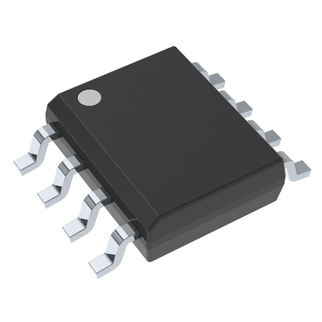
LP2989AIM-5.0/NOPB Equivalent & Substitute Parts
Part Overview
The LP2989AIM-5.0/NOPB is a linear voltage regulator IC from Texas Instruments designed for positive fixed 5V output applications with 500mA current capacity. This device operates in the Power Management (PMIC) category and is packaged in 8-SOIC format for surface mount applications. The part is currently in Last Time Buy status, indicating end-of-life production. Identifying equivalent and substitute parts is necessary to ensure design continuity, maintain supply chain flexibility, and support long-term product availability for applications requiring 5V regulation at 500mA output.
Substiute Parts
Key Parameters
| Parameter | LP2989AIM-5.0/NOPB |
|---|---|
| Output Voltage (Fixed) | 5V |
| Output Current | 500mA |
| Input Voltage (Max) | 16V |
| Voltage Dropout (Max) | 0.65V @ 500mA |
| Quiescent Current | 175 µA |
| Operating Temperature Range | -40°C ~ 125°C |
| Package Type | 8-SOIC (0.154", 3.90mm Width) |
| Control Features | Enable |
| Protection Features | Over Current, Over Temperature, Short Circuit |
| RoHS Status | ROHS3 Compliant |
| Moisture Sensitivity Level | 1 (Unlimited) |
Substitute Part Grouping Explanation
Substitution for the LP2989AIM-5.0/NOPB is determined by the following critical electrical and mechanical parameters:
- Fixed output voltage of 5V
- Output current capability of 500mA minimum
- Input voltage tolerance up to 16V or higher
- Operating temperature range of -40°C to 125°C
- Surface mount packaging compatibility
- RoHS3 compliance and MSL Level 1 rating
- Enable control feature for circuit management
The TPS7A2650DRVR qualifies as a manufacturer-recommended substitute based on matching these core parameters while offering improved electrical performance characteristics.
Parameter Comparison
| Parameter | LP2989AIM-5.0/NOPB | TPS7A2650DRVR | Compatibility Notes |
|---|---|---|---|
| Output Voltage (Fixed) | 5V | 5V | Identical |
| Output Current | 500mA | 500mA | Identical |
| Input Voltage (Max) | 16V | 18V | TPS7A2650DRVR supports higher input voltage |
| Voltage Dropout (Max) | 0.65V @ 500mA | 0.33V @ 500mA | TPS7A2650DRVR provides superior dropout performance |
| Quiescent Current | 175 µA | 4.5 µA | TPS7A2650DRVR significantly lower quiescent current |
| Operating Temperature Range | -40°C ~ 125°C | -40°C ~ 125°C (TJ) | Identical |
| Package Type | 8-SOIC | 6-WSON (2x2) | Different package; PCB layout modification required |
| Control Features | Enable | Enable, Power Good | TPS7A2650DRVR includes additional Power Good output |
| Protection Features | Over Current, Over Temperature, Short Circuit | Over Current, Over Temperature, UVLO | Both provide comprehensive protection; TPS7A2650DRVR adds UVLO |
| RoHS Status | ROHS3 Compliant | ROHS3 Compliant | Identical |
| Moisture Sensitivity Level | 1 (Unlimited) | 1 (Unlimited) | Identical |
Engineering Selection Recommendations
The TPS7A2650DRVR is the manufacturer-recommended substitute for the LP2989AIM-5.0/NOPB. Both devices maintain Active product status with full RoHS3 compliance and MSL Level 1 rating, ensuring regulatory and environmental compliance equivalence.
The primary consideration for substitution is the package change from 8-SOIC to 6-WSON (2x2). This requires PCB layout modification and footprint redesign. The electrical performance of the TPS7A2650DRVR exceeds the original part, with lower dropout voltage (0.33V vs. 0.65V) and significantly reduced quiescent current (4.5 µA vs. 175 µA), making it suitable for applications where power efficiency is a design priority.
The TPS7A2650DRVR provides additional control features including Power Good output and UVLO (Under-Voltage Lockout) protection, which may enhance system reliability in applications requiring voltage monitoring or supply sequencing.
Frequently Asked Questions (FAQ)
Q: Can the TPS7A2650DRVR directly replace the LP2989AIM-5.0/NOPB without PCB modifications?
A: No. The TPS7A2650DRVR uses a 6-WSON (2x2) package while the LP2989AIM-5.0/NOPB uses an 8-SOIC package. PCB footprint redesign and layout modification are required. Pin configuration and signal routing must be verified against device datasheets before implementation.
Q: What are the key electrical advantages of the TPS7A2650DRVR?
A: The TPS7A2650DRVR provides lower dropout voltage (0.33V vs. 0.65V at 500mA) and significantly lower quiescent current (4.5 µA vs. 175 µA). These characteristics reduce power dissipation and improve efficiency in battery-powered or thermally constrained applications.
Q: Are both parts compliant with the same regulatory standards?
A: Yes. Both the LP2989AIM-5.0/NOPB and TPS7A2650DRVR are ROHS3 compliant with MSL Level 1 rating, REACH unaffected status, and EAR99 ECCN classification.
Q: What is the significance of the Power Good output on the TPS7A2650DRVR?
A: The Power Good output provides a logic signal indicating when the regulated output voltage is within specification. This feature enables system-level voltage monitoring and supply sequencing, which may be beneficial for multi-rail power management applications.
Q: Does the higher input voltage rating of the TPS7A2650DRVR (18V vs. 16V) affect substitution compatibility?
A: The higher input voltage rating of the TPS7A2650DRVR (18V maximum) is compatible with applications designed for the LP2989AIM-5.0/NOPB (16V maximum). The substitute part provides additional margin for input voltage transients and supply variations.
Alternative Parts

SJ6012L2TP
Littelfuse Inc.
6 Alternative Parts

JMK107BBJ476MA-RE
Taiyo Yuden
10 Alternative Parts

GMK107BBJ475MA-T
Taiyo Yuden
5 Alternative Parts
SJ6020N2ARP
Littelfuse Inc.
3 Alternative Parts
SJ6025R2ATP
Littelfuse Inc.
4 Alternative Parts

2474-05L
API Delevan Inc.
1 Alternative Parts

4590R-684K
API Delevan Inc.
1 Alternative Parts

CM6560R-334
API Delevan Inc.
1 Alternative Parts

CM6460-104
API Delevan Inc.
1 Alternative Parts

5526-12
API Delevan Inc.
1 Alternative Parts