


Request Quote
(Ships tomorrow)
LMC7111BIN Equivalent & Substitute Parts
Part Overview
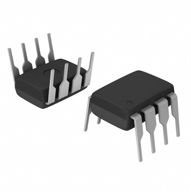
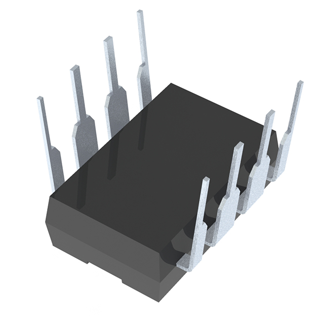
The LMC7111BIN is a general-purpose operational amplifier manufactured by Texas Instruments, featuring rail-to-rail output capability in an 8-PDIP through-hole package. This device is classified as obsolete, necessitating identification of functionally equivalent alternatives for ongoing design support and component procurement. The LMC7111BIN operates across a 2.5V to 11V supply range with a slew rate of 0.03V/µs and gain bandwidth product of 50 kHz, making it suitable for low-speed, low-power analog signal processing applications.
Substiute Parts
Key Parameters
| Parameter | LMC7111BIN |
|---|---|
| Amplifier Type | General Purpose |
| Number of Circuits | 1 |
| Output Type | Rail-to-Rail |
| Package / Case | 8-DIP (0.300", 7.62mm) |
| Mounting Type | Through Hole |
| Operating Temperature Range | -40°C ~ 85°C |
| Voltage - Supply Span (Min) | 2.5 V |
| Voltage - Supply Span (Max) | 11 V |
| Product Status | Obsolete |
Substitute Part Grouping Explanation
Substitution of the LMC7111BIN is determined by the following critical parameters that must be maintained or exceeded:
Package Compatibility: Both the main part and substitute must utilize the 8-DIP (0.300", 7.62mm) through-hole package to ensure direct PCB footprint compatibility without layout modifications.
Functional Architecture: Single-circuit operational amplifier configuration with rail-to-rail output capability is required to preserve signal swing characteristics in the application circuit.
Operating Temperature Range: The substitute must support the full -40°C to 85°C operating temperature range to maintain performance across the specified environmental conditions.
Supply Voltage Range: The substitute must operate within or encompass the 2.5V to 11V supply span of the original design. Substitutes with wider supply ranges are acceptable provided minimum and maximum ratings are not violated.
Single Circuit Count: The substitute must contain exactly one amplifier circuit to match the original device configuration and prevent unnecessary component proliferation in the design.
The AD820ANZ from Analog Devices Inc. satisfies all mandatory substitution criteria through equivalent package geometry, single-circuit architecture, rail-to-rail output, matching temperature range, and compatible supply voltage specifications.
Parameter Comparison
| Parameter | LMC7111BIN | AD820ANZ | Notes |
|---|---|---|---|
| Manufacturer | Texas Instruments | Analog Devices Inc. | Different manufacturers |
| Amplifier Type | General Purpose | J-FET | Different input stage architecture |
| Number of Circuits | 1 | 1 | Equivalent |
| Output Type | Rail-to-Rail | Rail-to-Rail | Equivalent |
| Slew Rate | 0.03 V/µs | 3 V/µs | AD820ANZ significantly higher |
| Gain Bandwidth Product | 50 kHz | 1.8 MHz | AD820ANZ significantly higher |
| Current - Input Bias | 0.1 pA | 2 pA | AD820ANZ higher input bias current |
| Voltage - Input Offset | 900 µV | 400 µV | AD820ANZ lower offset voltage |
| Current - Supply | 25 µA | 700 µA | AD820ANZ higher supply current |
| Current - Output / Channel | 30 mA | 20 mA | LMC7111BIN higher output current |
| Voltage - Supply Span (Min) | 2.5 V | 5 V | AD820ANZ requires higher minimum supply |
| Voltage - Supply Span (Max) | 11 V | 36 V | AD820ANZ supports wider range |
| Operating Temperature | -40°C ~ 85°C | -40°C ~ 85°C | Equivalent |
| Mounting Type | Through Hole | Through Hole | Equivalent |
| Package / Case | 8-DIP (0.300", 7.62mm) | 8-DIP (0.300", 7.62mm) | Equivalent |
| Product Status | Obsolete | Active | AD820ANZ actively manufactured |
| RoHS Status | RoHS non-compliant | ROHS3 Compliant | AD820ANZ meets current compliance |
Engineering Selection Recommendations
Product Status Consideration: The LMC7111BIN is classified as obsolete, while the AD820ANZ maintains active production status. Selection of the AD820ANZ ensures long-term component availability and supply chain continuity for new designs and production runs.
Compliance and Certification: The AD820ANZ is ROHS3 compliant, meeting current environmental and regulatory requirements. The LMC7111BIN is RoHS non-compliant, presenting potential procurement restrictions in regulated markets. Both devices are REACH Unaffected and classified under ECCN EAR99.
Package and Mounting Compatibility: Both devices utilize identical 8-DIP (0.300", 7.62mm) through-hole packaging, enabling direct substitution without PCB layout modifications or mechanical redesign.
Functional Equivalence: Both devices provide single-circuit, rail-to-rail operational amplifier functionality within the specified -40°C to 85°C operating temperature range. The AD820ANZ supply voltage minimum of 5V exceeds the LMC7111BIN minimum of 2.5V; applications operating below 5V supply voltage cannot use the AD820ANZ as a direct substitute.
Performance Characteristics: The AD820ANZ exhibits superior dynamic performance with slew rate of 3V/µs and gain bandwidth product of 1.8 MHz compared to the LMC7111BIN specifications of 0.03V/µs and 50 kHz. These enhanced characteristics do not preclude substitution in applications designed for the lower-performance original device. The AD820ANZ demonstrates lower input offset voltage (400µV versus 900µV) and higher supply current consumption (700µA versus 25µA).
Frequently Asked Questions (FAQ)
Q: Can the AD820ANZ directly replace the LMC7111BIN in all applications?
A: Direct substitution is possible only in applications where the supply voltage remains at or above 5V. The AD820ANZ minimum supply voltage of 5V exceeds the LMC7111BIN minimum of 2.5V. Applications operating at supply voltages between 2.5V and 5V require alternative solutions. Pin-for-pin compatibility and identical package geometry enable mechanical and electrical substitution for qualifying voltage ranges.
Q: What are the key differences between these two devices?
A: The primary differences are amplifier type (General Purpose versus J-FET input stage), product status (Obsolete versus Active), and performance specifications. The AD820ANZ provides higher slew rate, greater gain bandwidth product, lower input offset voltage, and wider maximum supply voltage range. The LMC7111BIN offers lower supply current consumption and higher output current capability. Both maintain rail-to-rail output and identical package specifications.
Q: Does the AD820ANZ require any circuit modifications for substitution?
A: No circuit modifications are required for pin-for-pin substitution when supply voltage requirements are met. The identical 8-DIP package and pin configuration enable direct replacement without PCB layout changes. However, the higher supply current of the AD820ANZ (700µA versus 25µA) may require verification of power supply capacity in current-limited applications.
Q: Are there any compliance advantages to using the AD820ANZ?
A: Yes. The AD820ANZ is ROHS3 compliant, meeting current environmental regulations. The LMC7111BIN is RoHS non-compliant, which may restrict procurement in regulated industries and markets with mandatory RoHS compliance requirements. Both devices are REACH Unaffected.
Q: What is the impact of the higher slew rate and bandwidth of the AD820ANZ?
A: The AD820ANZ slew rate of 3V/µs and gain bandwidth product of 1.8 MHz are significantly higher than the LMC7111BIN specifications. These enhanced characteristics enable faster signal processing and higher-frequency operation. In applications designed for the lower-performance LMC7111BIN, the AD820ANZ will not introduce incompatibility; the superior performance characteristics are simply not utilized. Applications requiring the specific low-speed characteristics of the LMC7111BIN should verify that the higher performance does not introduce unintended circuit behavior such as increased noise or stability concerns.
Q: Is the AD820ANZ available in the same packaging as the LMC7111BIN?
A: Yes. Both devices are packaged in 8-DIP (0.300", 7.62mm) through-hole configuration, enabling direct PCB footprint compatibility without layout modifications.
Q: What should be verified before implementing the AD820ANZ as a substitute?
A: Verify that the application supply voltage is at or above 5V to meet the AD820ANZ minimum supply specification. Confirm that the power supply can deliver the higher supply current of 700µA. Review circuit performance to ensure that the enhanced slew rate and bandwidth do not introduce unintended effects. Validate that the higher input bias current (2pA versus 0.1pA) does not impact circuit accuracy in high-impedance applications.
Alternative Parts

SJ6012L2TP
Littelfuse Inc.
6 Alternative Parts

JMK107BBJ476MA-RE
Taiyo Yuden
10 Alternative Parts

GMK107BBJ475MA-T
Taiyo Yuden
5 Alternative Parts
SJ6020N2ARP
Littelfuse Inc.
3 Alternative Parts
SJ6025R2ATP
Littelfuse Inc.
4 Alternative Parts

2474-05L
API Delevan Inc.
1 Alternative Parts

4590R-684K
API Delevan Inc.
1 Alternative Parts

CM6560R-334
API Delevan Inc.
1 Alternative Parts

CM6460-104
API Delevan Inc.
1 Alternative Parts

5526-12
API Delevan Inc.
1 Alternative Parts